M29F002 データシートの表示(PDF) - STMicroelectronics
部品番号
コンポーネント説明
メーカー
M29F002 Datasheet PDF : 29 Pages
| |||
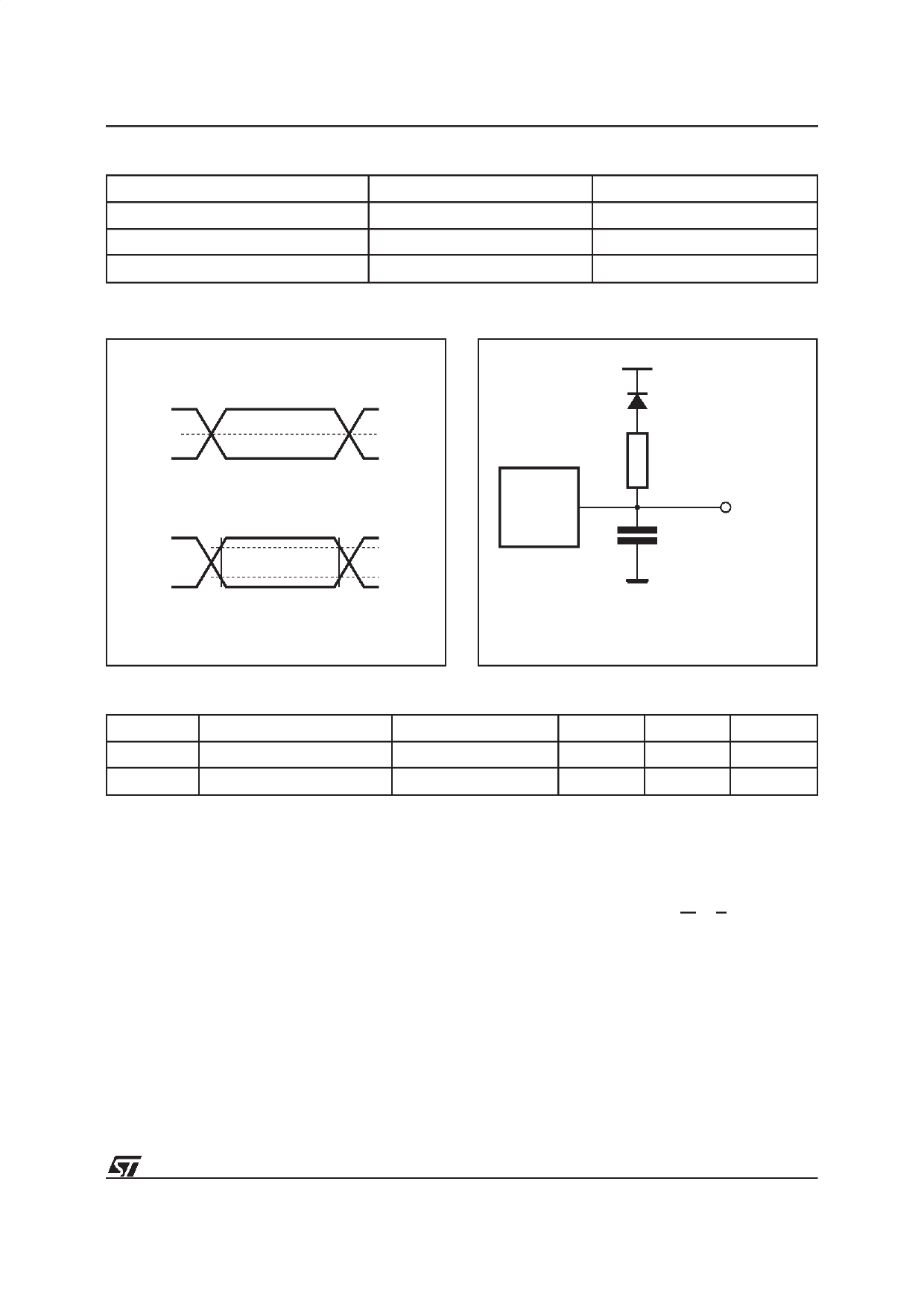
Table 11. AC Measurement Conditions
Input Rise and Fall Times
Input Pulse Voltages
Input and Output Timing Ref. Voltages
M29F002T, M29F002NT, M29F002B
High Speed
≤ 10ns
0 to 3V
1.5V
Standard
≤ 10ns
0.45V to 2.4V
0.8V and 2V
Figure 4. AC Testing Input Output Waveform
High Speed
3V
0V
Standard
2.4V
0.45V
1.5V
2.0V
0.8V
AI01275B
Figure 5. AC Testing Load Circuit
1.3V
1N914
DEVICE
UNDER
TEST
3.3kΩ
CL
OUT
CL = 30pF for High Speed
CL = 100pF for Standard
CL includes JIG capacitance
AI01276B
Table 12. Capacitance(1) (TA = 25 °C, f = 1 MHz )
Symbol
Parameter
Test Condition
CIN
Input Capacitance
VIN = 0V
C OUT
Output Capacitance
Note: 1. Sampled only, not 100% tested.
VOUT = 0V
Min
Max
Unit
6
pF
12
pF
Auto Select (AS) Instruction. This instruction
uses the two Coded cycles followed by one write
cycle giving the command 90h to address 555h for
command set-up. Asubsequentread will output the
manufacturer code and the device code or the
block protection status depending on the levels of
A0 and A1. The manufacturer code, 20h, is output
when the addresses lines A0 and A1 are Low, the
device code is output when A0 is High with A1 Low.
The AS instruction also allows access to the block
protectionstatus. After givingthe AS instruction, A0
is set to VIL with A1 at VIH, while A13-A17 define
the address of the block to be verified. A read in
these conditions will output a 01h if the block is
protected and a 00h if the block is not protected.
Program (PG) Instruction. This instruction uses
four write cycles. The Program command A0h is
written to address 555h on the third cycle after two
Coded cycles. A fourth write operation latches the
Address on the falling edge of W or E and the Data
to be written on the rising edge and starts the
P/E.C. Read operations output the Status Register
bits after the programming has started. Memory
programming is made only by writing ’0’ in place of
’1’. Status bits DQ6 and DQ7 determine if program-
ming is on-goingand DQ5 allows verification of any
possible error. Programming at an address not in
blocks being erased is also possible during erase
suspend. In this case, DQ2 will toggle at the ad-
dress being programmed.
11/29
Share Link: 