M29W008EB データシートの表示(PDF) - STMicroelectronics
部品番号
コンポーネント説明
メーカー
M29W008EB Datasheet PDF : 43 Pages
| |||
4 Command interface
M29W008ET, M29W008EB
Table 3. Commands
Command(1)
1st
Bus Write Operations(2)(3)
2nd
3rd
4th
5th
6th
7th
Add Data Add Data Add Data Add Data Add Data Add Data Add Data
Read/Reset(4)(5)
1
+
X
F0h
3
+
555h
AAh
2AAh
Read Memory Array until a new write cycle is initiated.
55h
555h
F0h
Read Memory Array until a new write cycle is
initiated.
Auto Select(5)
3
+
555h
AAh
2AAh
55h
555h
90h
Read Electronic Signature or Block Protection Status
until a new write cycle is initiated. (6)(7)
Program
4 555h AAh 2AAh 55h 555h A0h PA
PD
Read Data Polling or Toggle Bit until
Program completes.
Unlock Bypass 3 555h AAh 2AAh 55h 555h 20h
Unlock Bypass
Program
2
X
A0h
PA
PD
Unlock Bypass
Reset
2
X
90h
X
00h
Chip Erase
6 555h AAh 2AAh 55h 555h 80h 555h AAh 2AAh 55h 555h 10h
(8)
Block Erase
Erase
Suspend(10)
Erase Resume
6
+
555h
AAh
2AAh
55h
555h
80h
555h
AAh
2AAh
55h
BA
30h
AB
(9)
30h
1
X
B0h
Read until Toggle stops, then read all the data needed from any Block(s) not
being erased then Resume Erase.
1
X
30h
Read Data Polling or Toggle Bits until Erase completes or Erase is suspended
another time.
1. Commands not interpreted in this table will default to read array mode.
2. X = Don't Care. PA = Program Address, PD = Program Data, BA = Block Address, AB = Additional Block.
3. For Coded cycles address inputs A15-A19 are don't care.
4. A wait of tPLYH is necessary after a Read/Reset command if the memory was in an Erase or Program mode before starting
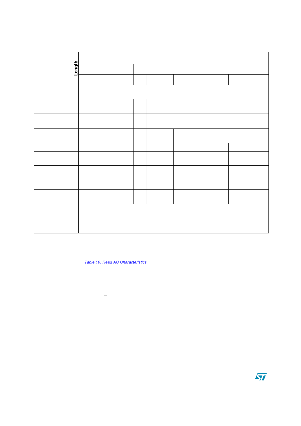
any new operation (see Table 10: Read AC Characteristics).
5. The first cycles of the Read/Reset and Auto Select commands are followed by read operations. Any number of read cycles
can occur after the command cycles.
6. Signature Address bits A0, A1, at VIL will output the Manufacturer Code (20h). Address bits A0 at VIH and A1, at VIL will
output the Device Code.
7. Block Protection Address: A0, at VIL, A1 at VIH and A13-A19 within the Block will output the Block Protection status.
8. Read Data Polling, Toggle bits or RB until Erase completes.
9. Optional, Additional Block (AB) addresses must be entered within the erase time-out delay after last write entry, time-out
status can be verified through DQ3 value (see Erase Timer Bit DQ3 description). When full command is entered, read Data
Polling or Toggle bit until Erase has completed or is suspended.
10. During Erase Suspend, Read and Data Program functions are allowed in blocks not being erased.
18/43
Share Link: 