PT6314-001L データシートの表示(PDF) - Princeton Technology
部品番号
コンポーネント説明
メーカー
PT6314-001L Datasheet PDF : 49 Pages
| |||
Tel: 886-2-66296288
Fax: 886-2-29174598
URL: http://www.princeton.com.tw
Dot Character VFD Controller/Driver IC
PT6314
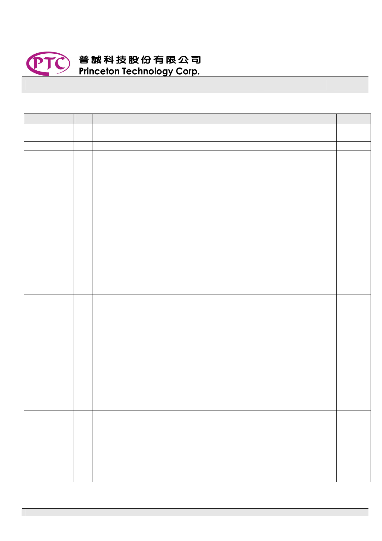
PIN DESCRIPTION
Pin Name
VDD2
VSS2
VDD1
OSCO
OSC2
OSC1
/RESET
TEST
DLS
DS1, DS0
R/W(/WR)
RS/STB
E(/RD)/SCK
I/O
Description
Pin No.
- VFD Driving Power Supply Pin
1, 36
- VFD Driving Power Supply Pin
2, 35
- Logic Power Supply Pin
3
O Oscillation Signal Output Pin
4
O Oscillation Output Pin
5
I Oscillation Input Pin
6
Reset Pin
I When this pin is set to “0”, all internal registers and commands are
7
initialized. The Segment and Grid Outputs are fixed to VDD.
Test Pin
I 0 or floating : the Normal Operation Mode
8
1:the Test Mode is active
Display Line Select Pin
I
This pin is used to select the number of display lines when
Power is ON, Reset or Resetting.
the
9
0: 1 line is selected (N=”0”)* 1: 2 lines are selected (N=”1”)*
Duty Select Pin
I These pins set the duty ratio. The duty ratio is determined by the
10, 11
number of Grid.
Read/Write (Write) Signal Pin
Under the M68 Parallel Data Transfer Mode (R/W), this pin functions as
the Data Transfer Select Pin.
I
0: Write Function 1: Read Function
Under the i80 parallel data Transfer Mode (/WR), this pin is Write
12
Enable Pin. It writes data at the rising edge of this signal.
Under the Serial Transfer Mode, the Read or Write function is selected
by instruction and this pin is connect to either “H” or “L”.
Register Select/Strobe Pin
Under the Parallel Transfer Mode is selected, this pin acts as the
I Register Select Pin.
13
0:Instruction Register (IR) 1: Data register (DR)
Under Serial Data Transfer Mode, this pin acts as the Strobe Input Pin.
Enable (Read)/Shift Clock
Under the M68 Parallel Data Transfer Mode (E), this pin functions as
the Write Enable Pin. Data is written at the falling edge.
I
Under the i80 Parallel Data Transfer Mode (/RD), this pin functions as
the Read Enable Pin. When this pin is set to “LOW”, data is outputted to
14
the Data Bus.
Under the Serial Data Transfer Mode, this pin functions as the Shift
Clock Input Pin. Data is written at the rising edge.
Note: *=N is the Display Line Select Flag in “Function Set” Command
PT6314 V1.3
-4-
March, 2006
Share Link: 