FDD3580 „Éá„Éľ„āŅ„ā∑„Éľ„Éą„ĀģŤ°®Á§ļÔľąPDFÔľČ - Fairchild Semiconductor
ťÉ®ŚďĀÁē™ŚŹ∑
„ā≥„É≥„ÉĚ„Éľ„Éć„É≥„ÉąŤ™¨śėé
„É°„Éľ„āę„Éľ
FDD3580 Datasheet PDF : 5 Pages
| |||
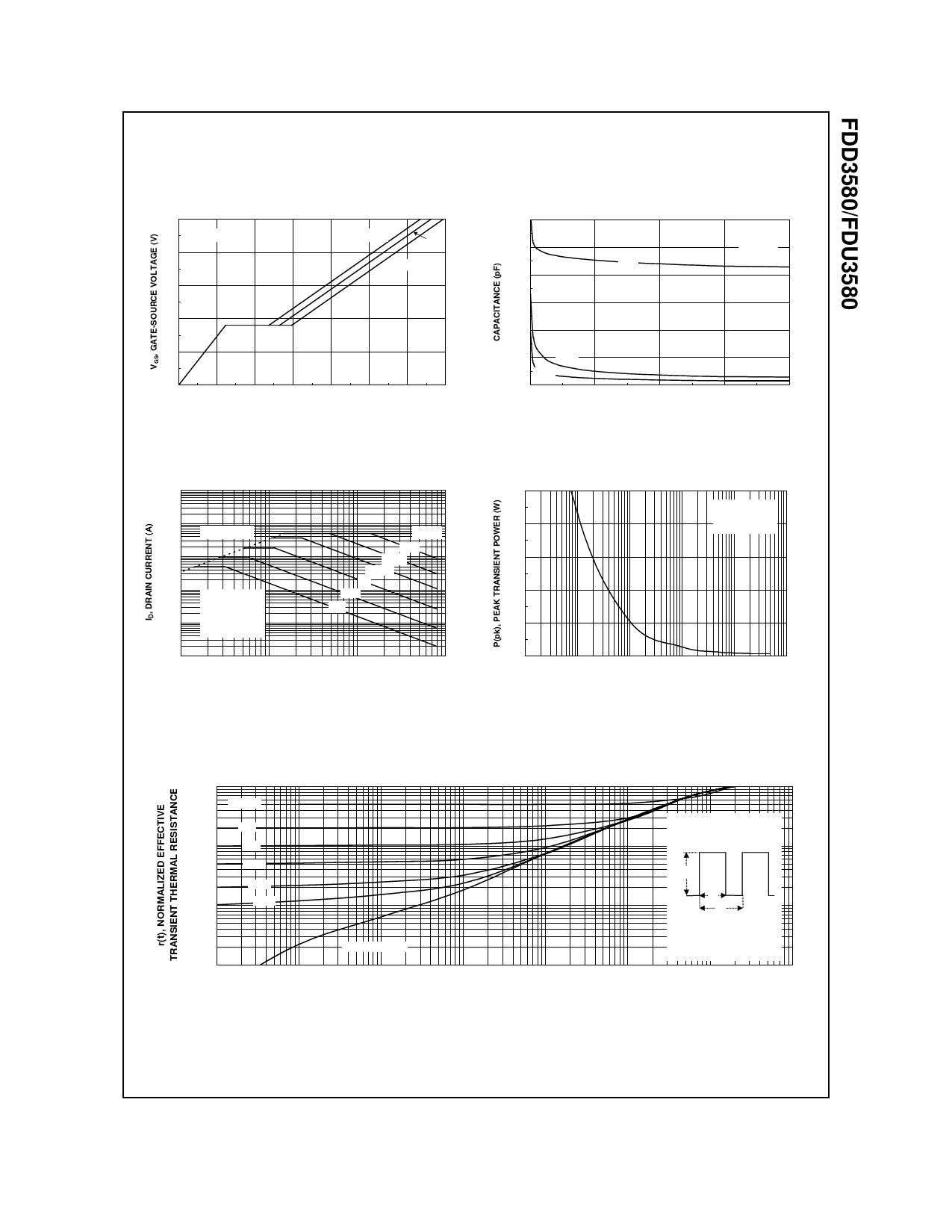
Typical Characteristics
10
ID = 7.7A
8
6
VDS = 10V
20V
40V
4
2
0
0
5
10
15
20
25
30
35
Qg, GATE CHARGE (nC)
Figure 7. Gate Charge Characteristics.
1000
100
RDS(ON) LIMIT
10
1
VGS = 10V
SINGLE PULSE
0.1
RőłJA = 96oC/W
TA = 25oC
100¬Ķs
1ms
10ms
100ms
1s
10s
DC
0.01
0.1
1
10
100
VDS, DRAIN-SOURCE VOLTAGE (V)
Figure 9. Maximum Safe Operating Area.
2400
2000
CISS
1600
f = 1MHz
VGS = 0 V
1200
800
400
COSS
CRSS
0
0
20
40
60
80
VDS, DRAIN TO SOURCE VOLTAGE (V)
Figure 8. Capacitance Characteristics.
100
80
60
40
20
0
0.01
0.1
SINGLE PULSE
RőłJA = 96¬įC/W
TA = 25¬įC
1
10
t1, TIME (sec)
100
1000
Figure 10. Single Pulse Maximum
Power Dissipation.
1
D = 0.5
0.2
0.1
0.1
RőłJA(t) = r(t) + RőłJA
RőłJA = 96 ¬įC/W
0.01
0.05
0.02
0.01
SINGLE PULSE
P(pk)
t1
t2
TJ - TA = P * RőłJA(t)
Duty Cycle, D = t1 / t2
0.001
0.0001
0.001
0.01
0.1
1
10
100
1000
Figure 11. Transient Thermal Response Curve.
Thermal characterization performed using the conditions described in Note 1b.
Transient thermal response will change depending on the circuit board design.
FDD3580/FDU3580 Rev. A1(W)
Share Link: 