S-8243AACFT-TB-G データシートの表示(PDF) - Seiko Instruments Inc
部品番号
コンポーネント説明
メーカー
S-8243AACFT-TB-G Datasheet PDF : 35 Pages
| |||
Rev.3.1_00
BATTERY PROTECTION IC FOR 3-SERIAL OR 4-SERIAL CELL PACK
S-8243A/B Series
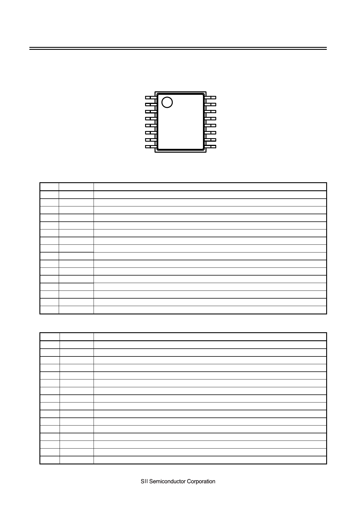
Pin Configuration
VDD
DOP
COP
VMP
VC1
VC2
VC3
VSS
16-Pin TSSOP
Top view
1
16
2
15
3
14
4
13
5
12
6
11
7
10
8
9
VREG
CTL1
CTL2
CTL3
CTL4
VBATOUT
CCT
CDT
Figure 3
Table 3 Pin description (S-8243A Series)
Pin No.
1
2
3
4
5
6
7
8
9
10
11
12
13
14
15
16
Symbol
VDD
DOP
COP
VMP
VC1
VC2
VC3
VSS
CDT
CCT
VBATOUT
CTL4
CTL3
CTL2
CTL1
VREG
Description
Input pin for positive power supply, Connection pin for battery 1’s positive voltage
Connection pin for discharge control FET gate (CMOS output)
Connection pin for charge control FET gate (Nch open drain output)
Pin for voltage detection between VDD-VMP pin (Pin for overcurrent detection)
No connection
Connection pin for battery 1’s negative voltage, for battery 2’s positive voltage
Connection pin for battery 2’s negative voltage, for battery 3’s positive voltage
Input pin for negative power supply, Connection pin for battery 3’s negative voltage
Connection pin to capacitor for overdischarge detection delay, for overcurrent detection delay 1
Connection pin to capacitor for overcharge detection delay
Output pin for battery voltage and offset voltage
Pin for selecting output from VBATOUT pin
Pin for selecting output from VBATOUT pin
Control pin for charge / discharge FET
Control pin for charge / discharge FET
Output pin for voltage regulator (3.3 V)
Table 4 Pin description (S-8243B Series)
Pin No.
1
2
3
4
5
6
7
8
9
10
11
12
13
14
15
16
Symbol
VDD
DOP
COP
VMP
VC1
VC2
VC3
VSS
CDT
CCT
VBATOUT
CTL4
CTL3
CTL2
CTL1
VREG
Description
Input pin for positive power supply, Connection pin for battery 1’s positive voltage
Connection pin for discharge control FET gate (CMOS output)
Connection pin for charge control FET gate (Nch open drain output)
Pin for voltage detection between VDD-VMP pin (Pin for overcurrent detection)
Connection pin for battery 1’s negative voltage, for battery 2’s positive voltage
Connection pin for battery 2’s negative voltage, for battery 3’s positive voltage
Connection pin for battery 3’s negative voltage, for battery 4’s positive voltage
Input pin for negative power supply, Connection pin for battery 4’s negative voltage
Connection pin to capacitor for overdischarge detection delay, for overcurrent detection delay 1
Connection pin to capacitor for overcharge detection delay
Output pin for battery voltage and offset voltage
Pin for selecting output from VBATOUT pin
Pin for selecting output from VBATOUT pin
Control pin for charge / discharge FET
Control pin for charge / discharge FET
Output pin for voltage regulator (3.3 V)
5
Share Link: 