SA9024 データシートの表示(PDF) - Philips Electronics
部品番号
コンポーネント説明
メーカー
SA9024 Datasheet PDF : 23 Pages
| |||
Philips Semiconductors
900 MHz transmit modulator and 1.3 GHz
fractional–N synthesizer
Objective specification
SA9024
power control, ÷M (offset loop), SE (Tx offset loop synthesizer
enable), DUAL mode, Sleep Mode 1 and Sleep Mode 2.
The data for FDAC is stored by the B word into a temporary register.
When the A word is loaded, the data in this temporary register is
loaded together with the A word into the work registers to avoid false
temporary main synthesizer output caused by changes in fractional
compensation.
The A word contains new data for the main divider. The A word is
loaded into the working registers only when a main divider
synchronization signal is active to avoid phase jumps when
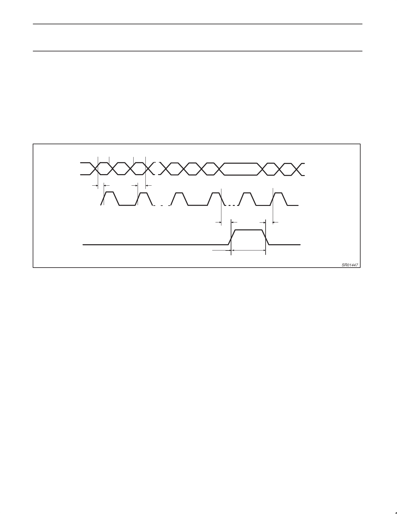
VALID DATA CHANGE
DATA
D0
D1
D21
tSU
tH
reprogramming the main divider. The synchronization pulse is
generated by the main divider when it has reached its terminal
count, at which time a main divider output pulse is also sent to the
main phase detector. This disables the loading of the A word each
main divider cycle during maximum of (NREF / ƒREF) seconds.
Therefore, to be sure that the A word will be correctly loaded, the
STROBE signal must be high for at least (NREF / ƒREF) seconds.
When programming the A word, the main charge pumps on output
PHP and PHI are set into the speed–up mode as soon as the A
word is latched into the working registers and remain so as long as
STROBE is held high.
D23
LAST
CLOCK
D0
FIRST
CLOCK
CLOCK
STROBE
CLOCK ENABLED–SHIFT IN DATA
tSU
tSU
CLOCK
DISABLED
STORE DATA
Figure 5. Serial Input Timing Sequence
SR01447
1997 Aug 01
11
Share Link: 