SI3233 „Éá„Éľ„āŅ„ā∑„Éľ„Éą„ĀģŤ°®Á§ļÔľąPDFÔľČ - Silicon Laboratories
ťÉ®ŚďĀÁē™ŚŹ∑
„ā≥„É≥„ÉĚ„Éľ„Éć„É≥„ÉąŤ™¨śėé
„É°„Éľ„āę„Éľ
SI3233 Datasheet PDF : 100 Pages
| |||
Si3233
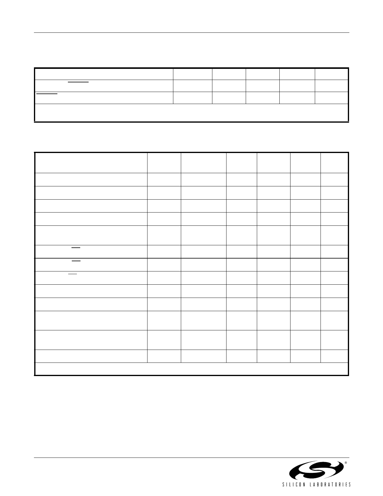
Table 9. Switching Characteristics‚ÄĒGeneral Inputs
VDDA = VDDA = 3.13 to 5.25 V, TA = 0 to 70¬įC for F-Grade, ‚Äď40 to 85¬įC for G-Grade, CL = 20 pF)
Parameter
Symbol
Min
Typ
Max
Unit
Rise Time, RESET
tr
‚ÄĒ
‚ÄĒ
20
ns
RESET Pulse Width
trl
100
‚ÄĒ
‚ÄĒ
ns
Note: All timing (except Rise and Fall time) is referenced to the 50% level of the waveform. Input test levels are
VIH = VD ‚Äď 0.4 V, VIL = 0.4 V. Rise and Fall times are referenced to the 20% and 80% levels of the waveform.
Table 10. Switching Characteristics‚ÄĒSPI
VDDA = VDDA = 3.13 to 5.25 V, TA = 0 to 70¬įC for F-Grade, ‚Äď40 to 85¬įC for G-Grade, CL = 20 pF
Parameter
Symbol
Test
Conditions
Min
Typ
Max
Unit
Cycle Time SCLK
tc
0.062
‚ÄĒ
‚ÄĒ
¬Ķs
Rise Time, SCLK
tr
‚ÄĒ
‚ÄĒ
25
ns
Fall Time, SCLK
tf
‚ÄĒ
‚ÄĒ
25
ns
Delay Time, SCLK Fall to SDO Active
td1
‚ÄĒ
‚ÄĒ
20
ns
Delay Time, SCLK Fall to SDO
td2
Transition
‚ÄĒ
‚ÄĒ
20
ns
Delay Time, CS Rise to SDO Tri-state
td3
‚ÄĒ
‚ÄĒ
20
ns
Setup Time, CS to SCLK Fall
tsu1
25
‚ÄĒ
‚ÄĒ
ns
Hold Time, CS to SCLK Rise
th1
20
‚ÄĒ
‚ÄĒ
ns
Setup Time, SDI to SCLK Rise
tsu2
25
‚ÄĒ
‚ÄĒ
ns
Hold Time, SDI to SCLK Rise
th2
20
‚ÄĒ
‚ÄĒ
ns
Delay Time between Chip Selects
tcs
(Continuous SCLK)
440
‚ÄĒ
‚ÄĒ
ns
Delay Time between Chip Selects
tcs
(Non-continuous SCLK)
220
‚ÄĒ
‚ÄĒ
ns
SDI to SDITHRU Propagation Delay
td4
‚ÄĒ
4
10
ns
Note: All timing is referenced to the 50% level of the waveform. Input test levels are VIH = VDDD ‚Äď0.4 V, VIL = 0.4 V
10
Preliminary Rev. 0.5
Share Link: 