SII141 データシートの表示(PDF) - Unspecified
部品番号
コンポーネント説明
メーカー
SII141 Datasheet PDF : 12 Pages
| |||
SiI 141B
SiI-DS-0037-C
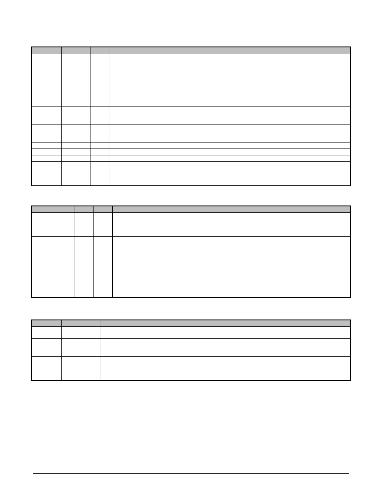
Output Pin Description
Pin Name
Q35 – Q0
Pin #
See
SiI 141B
Pin
Diagram
Type
Out
ODCK
DE
HSYNC
VSYNC
CTL1
CTL2
CTL3
36
Out
41
Out
12
Out
14
Out
8
Out
9
Out
10
Out
Description
Output Data [35:0].
Output data is synchronized with output data clock (ODCK).
When PIXS is low Q35-Q24 are low and Q23-Q0 output 24-bit/pixel data.
When PIXS is high Q17-Q0 output the even numbered pixels (pixel 0, 2, 4, ... , etc.) and Q35-Q18 output
the odd numbered pixels (pixel 1, 3, 5, ... , etc.).
Refer to the TFT Signal Mapping (SiI/AN-0008) and DSTN Signal Mapping (SiI/AN-0007) application notes
which tabulate the relationship between the input data to the transmitter and output data from the receiver.
A low level on PD or PDO will put the output drivers into a high impedance (tri-state) mode. A weak
internal pull-down device brings each output to ground.
Output Data Clock.
A low level on PD or PDO will put the output drivers into a high impedance (tri-state) mode. A weak
internal pull-down device brings each output to ground.
Output Data Enable.
A low level on PD or PDO will put the output drivers into a high impedance (tri-state) mode. A weak
internal pull-down device brings each output to ground.
Horizontal Sync output control signal.
Vertical Sync output control signal.
General output control signal 1. This pin is not controlled by PDO.
General output control signal 2
General output control signal 3.
A low level on PD or PDO will put the output drivers into a high impedance (tri-state) mode. A weak
internal pull-down device brings each output to ground.
Configuration Pin Description
Pin Name
OCK_INV
Pin #
80
Type
In
Description
ODCK Polarity. A low level selects normal ODCK output, which enables data latching on the falling
edge. A high level (3.3V) selects inverted ODCK output, which enables data latching on the rising edge.
Both conditions are for color TFT panel support. For color 24-bit DSTN panel support, please refer to the
DSTN Signal Mapping (SiI/AN-0008-A) application note.
PIXS
5
DF0
6
HSYNC_DEJTR 75
ST
79
In Pixel Select. A low level indicates that output data is one pixel (up to 24-bit) per clock and a high level
(3.3V) indicates that output data is two pixels (up to 36-bit) per clock.
In Output Data Format. This pin controls clock and data output format. A low level indicates that ODCK
runs continuously for color TFT panel support and a high level (3.3V) indicates that ODCK is stopped
(LOW) for color 24-bit DSTN panel support when DE is low. Refer to the TFT Signal Mapping (SiI/AN-
0007-A) and DSTN Signal Mapping (SiI/AN-0008-A) application notes for a table on TFT or DSTN panel
support.
In A low level enables the HSYNC de-jitter circuitry. A high level disables the de-jitter circuitry. If left
unconnected, the circuitry defaults to disabled.
In Output Driver Strength. A low level indicates low drive. A high level indicates high drive.
Power Management Pin Description
Pin Name Pin # Type Description
SCDT
7
Out SyncDetect. A high level is output when DE is toggling. A low level is output when DE is inactive. See page
9.
PD
2
In Power Down (active low). A high level (3.3V) indicates normal operation and a low level indicates power down
mode. During power down mode all internal circuitry is powered down and digital I/O are set the same as
when PDO is asserted. (see PDO pin description).
PDO
3
In Power Down Output (active low). A high level indicates normal operation. A low level puts the output drivers
only into a high impedance (tri-state) mode. A weak internal pull-down device brings each output to ground.
There is an internal pull-up resistor on PDO that defaults the chip to normal operation if left unconnected.
SCDT and CTL1 are not tri-stated by this pin. See explanation of clock detect on page 8-9.
Silicon Image, Inc.
7
Subject to Change without Notice
Share Link: 