SST49LF004B データシートの表示(PDF) - Silicon Storage Technology
部品番号
コンポーネント説明
メーカー
SST49LF004B Datasheet PDF : 36 Pages
| |||
EOL Data Sheet
Lock Down: The Lock-Down bit, bit 1, controls the
Block Locking registers. The default Lock Down status of
all blocks upon power-up is not locked down. Once the
Lock-Down bit is set, any future attempted changes to
that Block Locking register will be ignored. The Lock-
Down bit is only cleared upon a device reset with RST# or
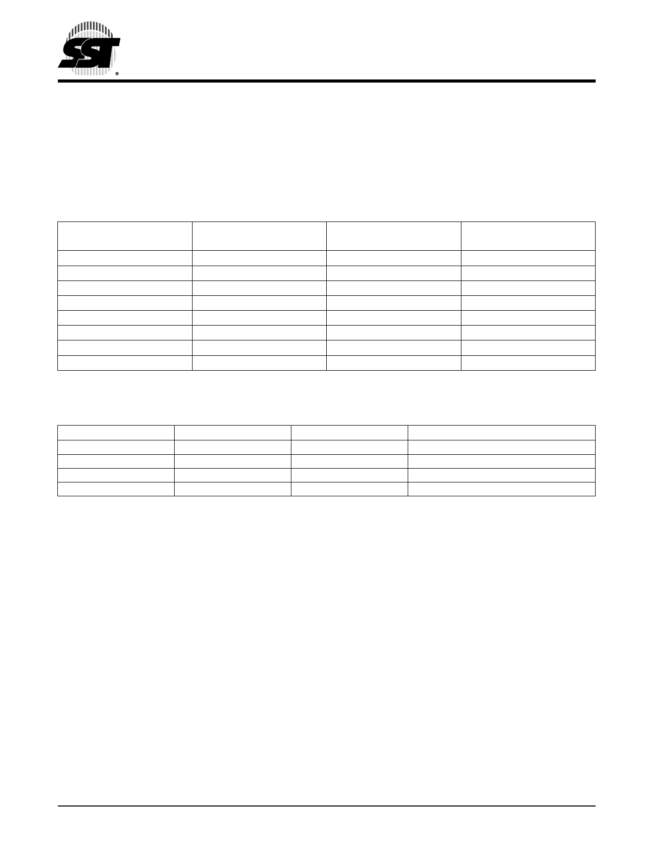
TABLE 7: BLOCK LOCKING REGISTERS1
Register
T_BLOCK_LK
T_MINUS01_LK
T_MINUS02_LK
T_MINUS03_LK
T_MINUS04_LK
T_MINUS05_LK
T_MINUS06_LK
T_MINUS07_LK
1. Default value at power up is 01H
Block Size
64K
64K
64K
64K
64K
64K
64K
64K
4 Mbit Firmware Hub
SST49LF004B
INIT# or power down. Current Lock Down status of a par-
ticular block can be determined by reading the corre-
sponding Lock-Down bit.
Once the Lock-Down bit of a block is set, the Write-Lock
bits for that block can no longer be modified, and the block
is locked down in its current state of write accessibility.
Protected Memory
Address Range
07FFFFH - 070000H
06FFFFH - 060000H
05FFFFH - 050000H
04FFFFH - 040000H
03FFFFH - 030000H
02FFFFH - 020000H
01FFFFH - 010000H
00FFFFH - 000000H
Memory Map
Register Address
FFBF0002H
FFBE0002H
FFBD0002H
FFBC0002H
FFBB0002H
FFBA0002H
FFB90002H
FFB80002H
T7.0 1307
TABLE 8: BLOCK LOCKING REGISTER BITS
Reserved Bit [7..2]
000000
000000
000000
000000
Lock-Down Bit [1]
0
0
1
1
Write-Lock Bit [0]
0
1
0
1
JEDEC ID Registers
The JEDEC ID registers provide access to the manufac-
turer and device ID information with a single Read cycle.
The JEDEC ID registers for the boot device appear at
FFBC0000H and FFBC0001H in the 4 GByte system
memory map, and will appear elsewhere if the device is not
the boot device. Registers are not available for read when
the device is in Erase/Program operation. Unused register
location will read as 00H. Refer to Table 2 for product identi-
fication information.
Lock Status
Full Access
Write Locked (Default State at Power-Up)
Locked Open (Full Access Locked Down)
Write Locked Down
T8.0 1307
©2007 Silicon Storage Technology, Inc.
16
S71307-03-EOL
12/07
Share Link: 