SST49LF004B データシートの表示(PDF) - Silicon Storage Technology
部品番号
コンポーネント説明
メーカー
SST49LF004B Datasheet PDF : 36 Pages
| |||
EOL Data Sheet
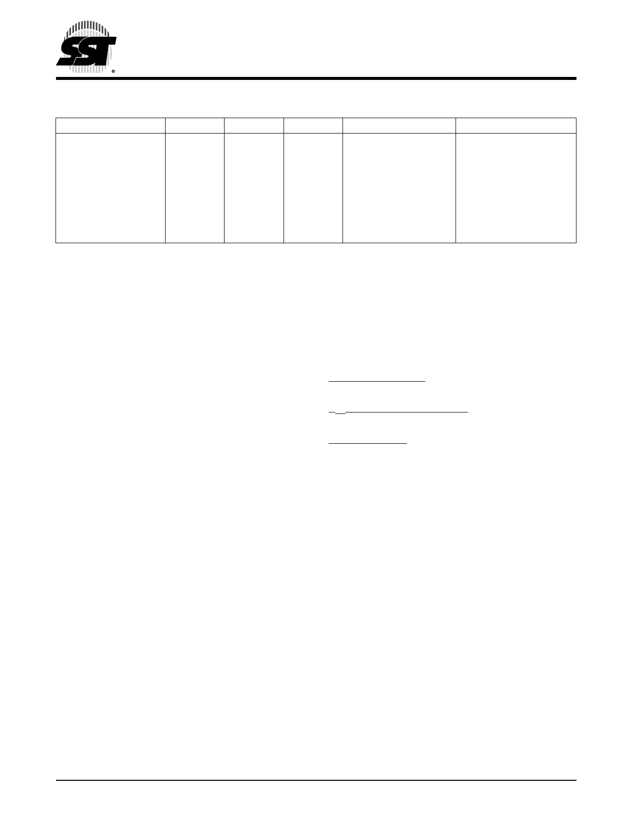
TABLE 9: OPERATION MODES SELECTION (PP MODE)
Mode
Read
Program
Erase
RST#
VIH
VIH
VIH
OE#
VIL
VIH
VIH
WE#
VIH
VIL
VIL
Reset
VIL
X
X
Write Inhibit
VIH
VIL
VIH
Product Identification
VIH
VIL
VIH
1. X can be VIL or VIH, but no other value.
2. Device ID = 60H for SST49LF004B
4 Mbit Firmware Hub
SST49LF004B
DQ
DOUT
DIN
X1
High Z
High Z/DOUT
Manufacturer’s ID (BFH)
Device ID2
Address
AIN
AIN
Sector or Block address,
XXH for Chip-Erase
X
X
A18 - A1 = VIL, A0 = VIL
A18 - A1 = VIL, A0 = VIH
T9.0 1307
Data# Polling DQ7
When the SST49LF004B device is in the internal Program
operation, any attempt to read DQ7 will produce the com-
plement of the true data. Once the Program operation is
completed, DQ7 will produce true data. Note that even
though DQ7 may have valid data immediately following the
completion of an internal Write operation, the remaining
data outputs may still be invalid. Valid data will appear on
the entire data bus in subsequent successive Read cycles
after an interval of 1 µs. During an internal Erase operation,
any attempt to read DQ7 will produce a '0'. Once the inter-
nal Erase operation is completed, DQ7 will produce a '1'.
Data# Polling is valid after the rising edge of the fourth WE#
pulse for the Program operation. For Sector-Erase, Block-
Erase, or Chip-Erase, the Data# Polling is valid after the ris-
ing edge of the sixth WE# pulse. See Figure 13 for Data#
Polling timing diagram. Proper status will not be given using
Data# Polling if the address is in the invalid range.
Toggle Bit DQ6
During the internal Program or Erase operation, any con-
secutive attempts to read DQ6 will produce alternating '0's
and '1's, i.e., toggling between 0 and 1. When the internal
Program or Erase operation is completed, the toggling will
stop. The device is then ready for the next operation. The
Toggle Bit is valid after the rising edge of the fourth WE#
pulse for Program operation. For Sector-Erase, Block-
Erase or Chip-Erase, the Toggle Bit is valid after the rising
edge of the sixth WE# pulse. See Figure 14 for Toggle Bit
timing diagram.
Data Protection (PP Mode)
The SST49LF004B device provides both hardware and
software features to protect nonvolatile data from inadvert-
ent writes.
Hardware Data Protection
Noise/Glitch Protection: A WE# pulse of less than 5 ns will
not initiate a Write cycle.
VDD Power Up/Down Detection: The Write operation is
inhibited when VDD is less than 1.5V.
Write Inhibit Mode: Forcing OE# low, WE# high will inhibit
the Write operation. This prevents inadvertent writes during
power-up or power-down.
Software Data Protection (SDP)
The SST49LF004B provides the JEDEC approved Soft-
ware Data Protection scheme for all data alteration opera-
tion, i.e., Program and Erase. Any Program operation
requires the inclusion of a series of three-byte sequence.
The three-byte load sequence is used to initiate the Pro-
gram operation, providing optimal protection from inadvert-
ent Write operations, e.g., during the system power-up or
power down. Any Erase operation requires the inclusion of
a five-byte load sequence.
©2007 Silicon Storage Technology, Inc.
18
S71307-03-EOL
12/07
Share Link: 