M80C186 データシートの表示(PDF) - Intel
部品番号
コンポーネント説明
メーカー
M80C186 Datasheet PDF : 59 Pages
| |||
M80C186
This input must satisfy set-up and hold times to guar-
antee proper operation of the circuit
In addition the M80C186 as part of the integrated
chip-select logic has the capability to program WAIT
states for memory and peripheral blocks This is dis-
cussed in the Chip Select Ready Logic description
RESET Logic
The M80C186 provides both a RES input pin and a
synchronized RESET pin for use with other system
components The RES input pin on the M80C186 is
provided with hysteresis in order to facilitate power-
on Reset generation via an RC network RESET is
guaranteed to remain active for at least five clocks
given a RES input of at least six clocks RESET may
be delayed up to two and one-half clocks behind
RES
Multiple M80C186 processors may be synchronized
through the RES input pin since this input resets
both the processor and divide-by-two internal coun-
ter in the clock generator In order to insure that the
divide-by-two counters all begin counting at the
same time the active going edge of RES must satis-
fy a 25 ns setup time before the falling edge of the
M80C186 clock input In addition in order to insure
that all CPUs begin executing in the same clock cy-
cle the reset must satisfy a 15 ns setup time before
the rising edge of the CLKOUT signal of all the proc-
essors
LOCAL BUS CONTROLLER
The M80C186 provides a local bus controller to gen-
erate the local bus control signals In addition it em-
ploys a HOLD HLDA protocol for relinquishing the
local bus to other bus masters It also provides con-
trol lines that can be used to enable external buffers
and to direct the flow of data on and off the local
bus
Memory Peripheral Control
The M80C186 provides ALE RD and WR bus con-
trol signals The RD and WR signals are used to
strobe data from memory to the M80C186 or to
strobe data from the M80C186 to memory The ALE
line provides a strobe to address latches for the mul-
tiplexed address data bus The M80C186 local bus
controller does not provide a memory I O signal If
this is required the user will have to use the S2 sig-
nal (which will require external latching) make the
memory and I O spaces nonoverlapping or use only
the integrated chip-select circuitry
Transceiver Control
The M80C186 generates two control signals to be
connected to external transceiver chips This capa-
bility allows the addition of transceivers for extra
buffering without adding external logic These con-
trol lines DT R and DEN are generated to control
the flow of data through the transceivers The opera-
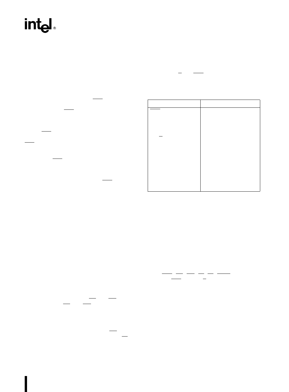
tion of these signals is shown in Table 6
Table 6 Transceiver Control Signals Description
Pin Name
Function
DEN (Data Enable)
DT R (Data Transmit
Receive)
Enables the output
drivers of the
transceivers It is active
LOW during memory
I O or INTA cycles
Determines the direction
of travel through the
transceivers A HIGH
level directs data away
from the processor
during write operations
while a LOW level directs
data toward the
processor during a read
operation
Local Bus Arbitration
The M80C186 uses a HOLD HLDA system of local
bus exchange This provides an asynchronous bus
exchange mechanism This means multiple masters
utilizing the same bus can operate at separate clock
frequencies The M80C186 provides a single HOLD
HLDA pair through which all other bus masters may
gain control of the local bus This requires external
circuitry to arbitrate which external device will gain
control of the bus from the M80C186 when there is
more than one alternate local bus master When the
M80C186 relinquishes control of the local bus it
floats DEN RD WR S0 –S2 LOCK AD0 – AD15
A16 – A19 BHE and DT R to allow another master
to drive these lines directly
The M80C186 HOLD latency time i e the time be-
tween HOLD request and HOLD acknowledge is a
function of the activity occurring in the processor
when the HOLD request is received A HOLD re-
quest is the highest-priority activity request which
the processor may receive higher than instruction
fetching or internal DMA cycles However if a DMA
cycle is in progress the M80C186 will complete the
transfer before relinquishing the bus This implies
that if a HOLD request is received just as a DMA
transfer begins the HOLD latency time can be as
great as 4 bus cycles This will occur if a DMA word
transfer operation is taking place from an odd ad-
19
Share Link: 