M80C186 データシートの表示(PDF) - Intel
部品番号
コンポーネント説明
メーカー
M80C186 Datasheet PDF : 59 Pages
| |||
M80C186
The user should program bits 15–6 to correspond to
the desired peripheral base location PACS bits 0– 2
are used to specify READY mode for PCS0 –PCS3
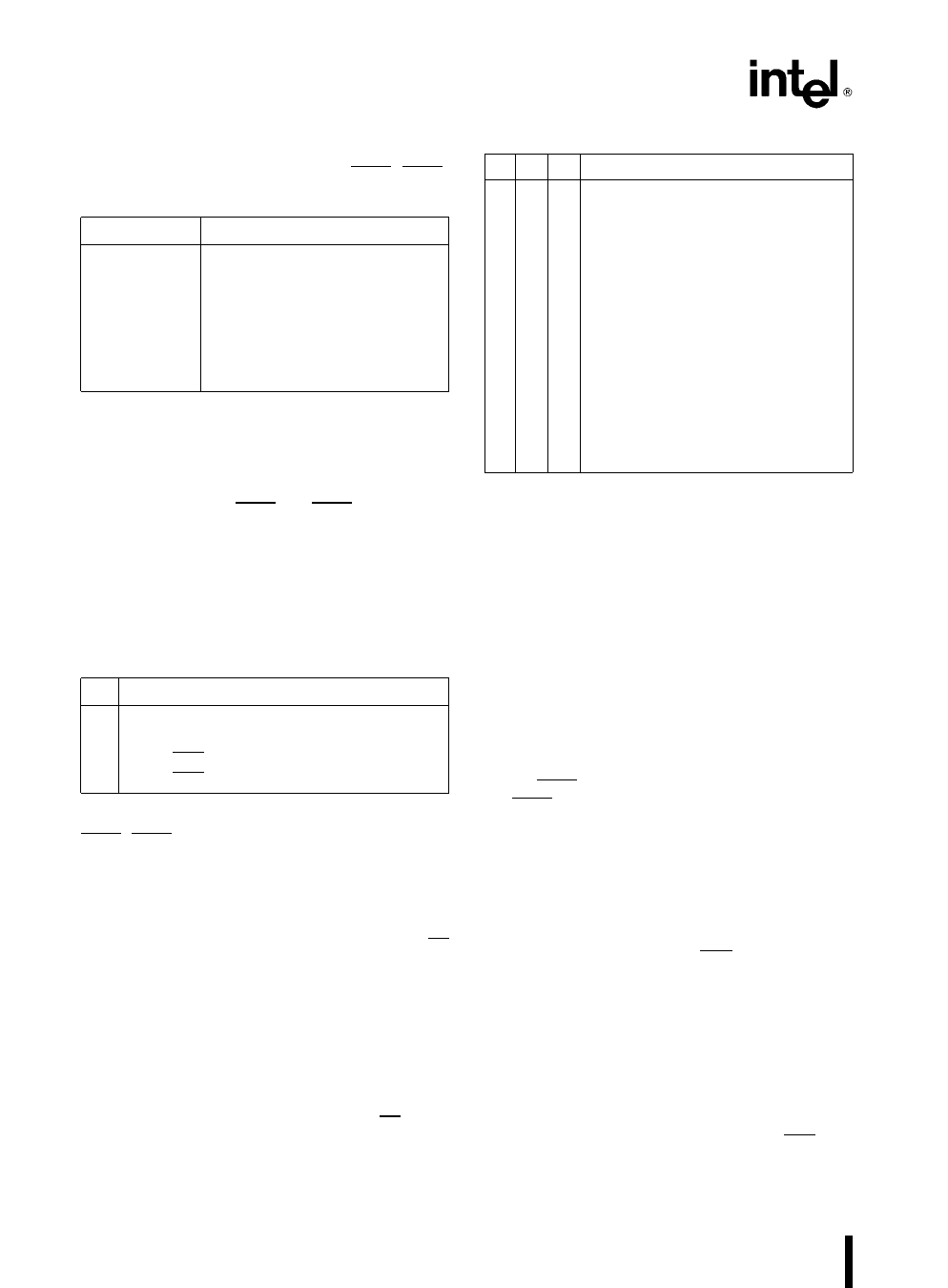
Table 10 PCS Address Ranges
PCS Line
Active between Locations
PCS0
PCS1
PCS2
PCS3
PCS4
PCS5
PCS6
PBA
PBAa128
PBAa256
PBAa384
PBAa512
PBAa640
PBAa768
PBAa127
PBAa255
PBAa383
PBAa511
PBAa639
PBAa767
PBAa895
The mode of operation of the peripheral chip selects
is defined by the MPCS register (which is also used
to set the size of the mid-range memory chip-select
block see Figure 13) This register is located at off-
set A8H in the internal control block Bit 7 is used to
select the function of PCS5 and PCS6 while bit 6 is
used to select whether the peripheral chip selects
are mapped into memory or I O space Table 11
describes the programming of these bits After reset
the contents of both the MPCS and the PACS regis-
ters are undefined however none of the PCS lines
will be active until both of the MPCS and PACS reg-
isters are accessed
Table 11 MS EX Programming Values
Bit
Description
MS 1 e Peripherals mapped into memory space
0 e Peripherals mapped into I O space
EX 0 e 5 PCS lines A1 A2 provided
1 e 7 PCS lines A1 A2 are not provided
MPCS bits 0– 2 are used to specify READY mode for
PCS4–PCS6 as outlined below
READY Generation Logic
The M80C186 can generate a ‘‘READY’’ signal in-
ternally for each of the memory or peripheral CS
lines The number of WAIT states to be inserted for
each peripheral or memory is programmable to pro-
vide 0–3 wait states for all accesses to the area for
which the chip select is active In addition the
M80C186 may be programmed to either ignore ex-
ternal READY for each chip-select range individually
or to factor external READY with the integrated
ready generator
READY control consists of 3 bits for each CS line or
group of lines generated by the M80C186 The inter-
pretation of the ready bits is shown in Table 12
Table 12 READY Bits Programming
R2 R1 R0 Number of WAIT States Generated
0 0 0 0 wait states external RDY
also used
0 0 1 1 wait state inserted external RDY
also used
0 1 0 2 wait states inserted external RDY
also used
0 1 1 3 wait states inserted external RDY
also used
1 0 0 0 wait states external RDY
ignored
1 0 1 1 wait state inserted external RDY
ignored
1 1 0 2 wait states inserted external RDY
ignored
1 1 1 3 wait states inserted external RDY
ignored
The internal ready generator operates in parallel
with external READY not in series if the external
READY is used (R2 e 0) This means for example
if the internal generator is set to insert two wait
states but activity on the external READY lines will
insert four wait states the processor will only insert
four wait states not six This is because the two wait
states generated by the internal generator over-
lapped the first two wait states generated by the ex-
ternal ready signal Note that the external ARDY and
SRDY lines are always ignored during cycles ac-
cessing internal peripherals
R2– R0 of each control word specifies the READY
mode for the corresponding block with the excep-
tion of the peripheral chip selects R2 – R0 of PACS
set the PCS0– 3 READY mode R2 – R0 of MPCS set
the PCS4 – 6 READY mode
Chip Select Ready Logic and Reset
Upon reset the Chip-Select Ready Logic will per-
form the following actions
All chip-select outputs will be driven HIGH
Upon leaving RESET the UCS line will be pro-
grammed to provide chip selects to a 1K block
with the accompanying READY control bits set at
011 to allow the maximum number of internal wait
states in conjunction with external Ready consid-
eration (i e UMCS resets to FFFBH)
No other chip select or READY control registers
have any predefined values after RESET They
will not become active until the CPU accesses
their control registers Both the PACS and MPCS
registers must be accessed before the PCS lines
will become active
24
Share Link: 