TFRA08C13 データシートの表示(PDF) - Agere -> LSI Corporation
部品番号
コンポーネント説明
メーカー
TFRA08C13 Datasheet PDF : 188 Pages
| |||
TFRA08C13 OCTAL T1/E1 Framer
Preliminary Data Sheet
October 2000
Pin Information (continued)
Table 1. Pin Assignments for 352-Pin PBGA by Pin Number Order (continued)
Pin Signal Name
AE5 DS1/CEPT3
AE6 A2
AE7 A6
AE8 A9
AE9 SECOND
AE10 MPCLK
AE11 RCHIDATAB4
AE12 TFDLCK4
AE13 TFS4
AE14 AD1
AE15 AD5
AE16 AD7
Pin Signal Name
AE17 RFDLCK4
AE18 RFRMDATA4
AE19 NC
AE20 TND4
AE21 VSS
AE22 TPD5
AE23 NC
AE24 NC
AE25 NC
AE26 TLCK5
AF1 NC
AF2 RFRMCLK3
Pin Signal Name
AF3 VDD
AF4 RLCK3
AF5 VDD
AF6 A5
AF7 A7
AF8 A11
AF9 MPMODE
AF10 RPD4
AF11 TFDL4
AF12 TCRCMFS4
AF13 TCHIDATA4
AF14 AD3
Pin Signal Name
AF15 AD6
AF16 NC
AF17 RSSFS4
AF18 NC
AF19 TLCK4
AF20 RLCK4
AF21 RLCK5
AF22 TND5
AF23 NC
AF24 NC
AF25 NC
AF26 NC
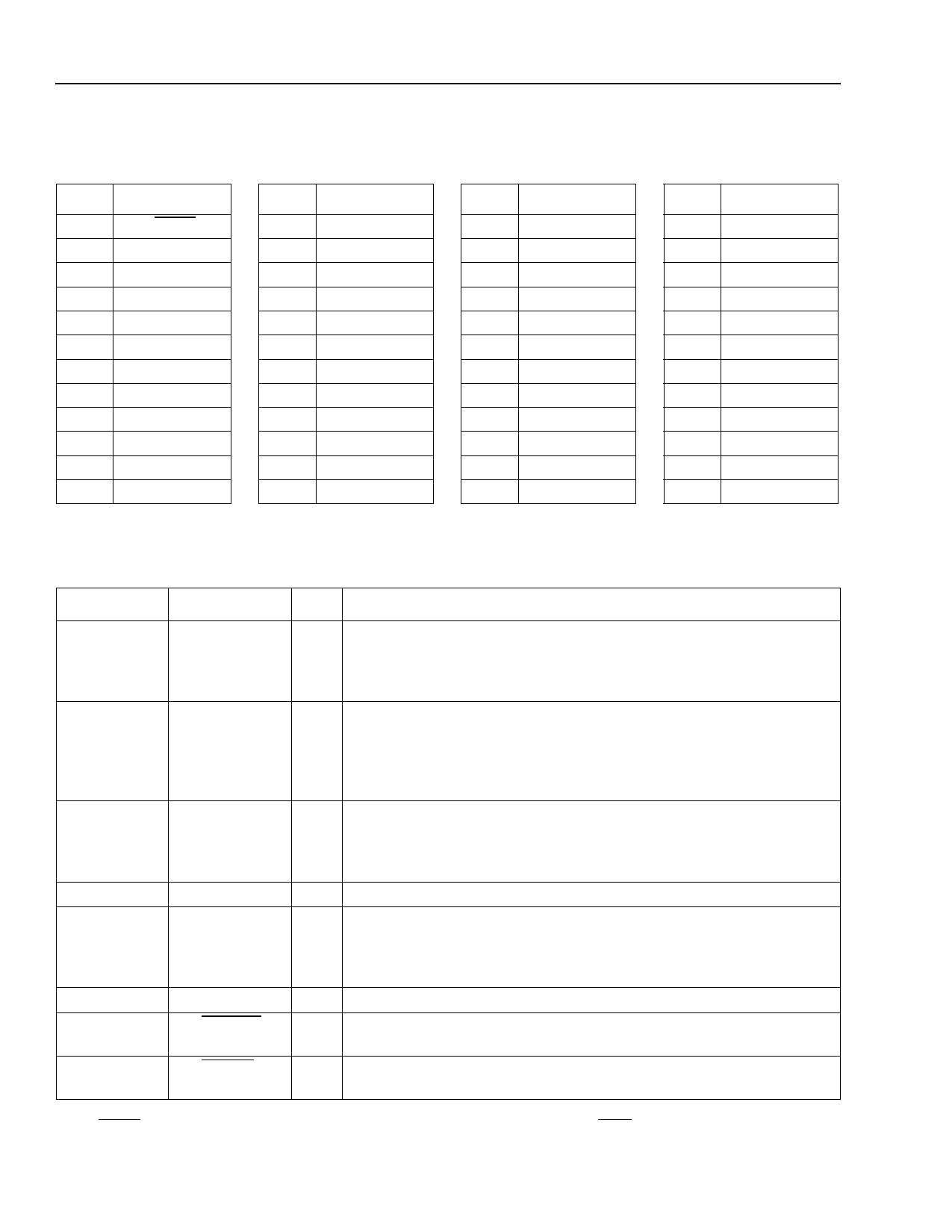
Table 2 shows the list of the TFRA08C13 pins and a functional description for each.
Table 2. Pin Descriptions
Pins
Symbol Type*
Description
AF3, AF5,
VDD
AD18, K25,
E24, K4,
M2, U3
P 3.3 V Power Supply. 3.3 V ± 5%. Each of these pins must be bypassed
with a 0.1 µF capacitor to VSS, as close to the pin as possible.
AD20, AD26,
VSS
AE21, G3,
K24,
A18, J3, C7,
Y2
G Ground.
D17
VDDA
P 3.3 V Quiet Analog Power Supply. This pin must be bypassed with a
0.1 µF capacitor to VSSA, as close to the pin as possible. In addition,
this pin should be isolated from the 3.3 V power plane with an inductive
bead.
C17
VSSA
G 3.3 V Quiet Analog Ground.
A14
VDDD
P 3.3 V Quiet Digital Power Supply. This pin must be bypassed with a
0.1 µF capacitor to VSSD, as close to the pin as possible. In addition,
this pin should be isolated from the 3.3 V power plane with an inductive
bead.
A13
VSSD
G 3.3 V Quiet Digital Ground.
B18
3-STATE
Iu 3-State (Active-Low). Asserting this pin low forces the channel outputs
into a high-impedance state.
C19
RESET†
Iu Reset (Active-Low). Asserting this pin low resets all channels on the
entire device.
* Iu indicates an internal pull-up, Id indicates an internal pull-down.
† After RESET is deasserted, the channel is in the default framing mode, as a function of the DS1/CEPT pin.
‡ Asserting this pin low will initially force RDY to a low state.
18
LuLcuecnetnTteTcehcnhonloolgoigeisesInIcn.c.
Share Link: 