TGA4522 データシートの表示(PDF) - TriQuint Semiconductor
部品番号
コンポーネント説明
メーカー
TGA4522 Datasheet PDF : 12 Pages
| |||
TGA4522
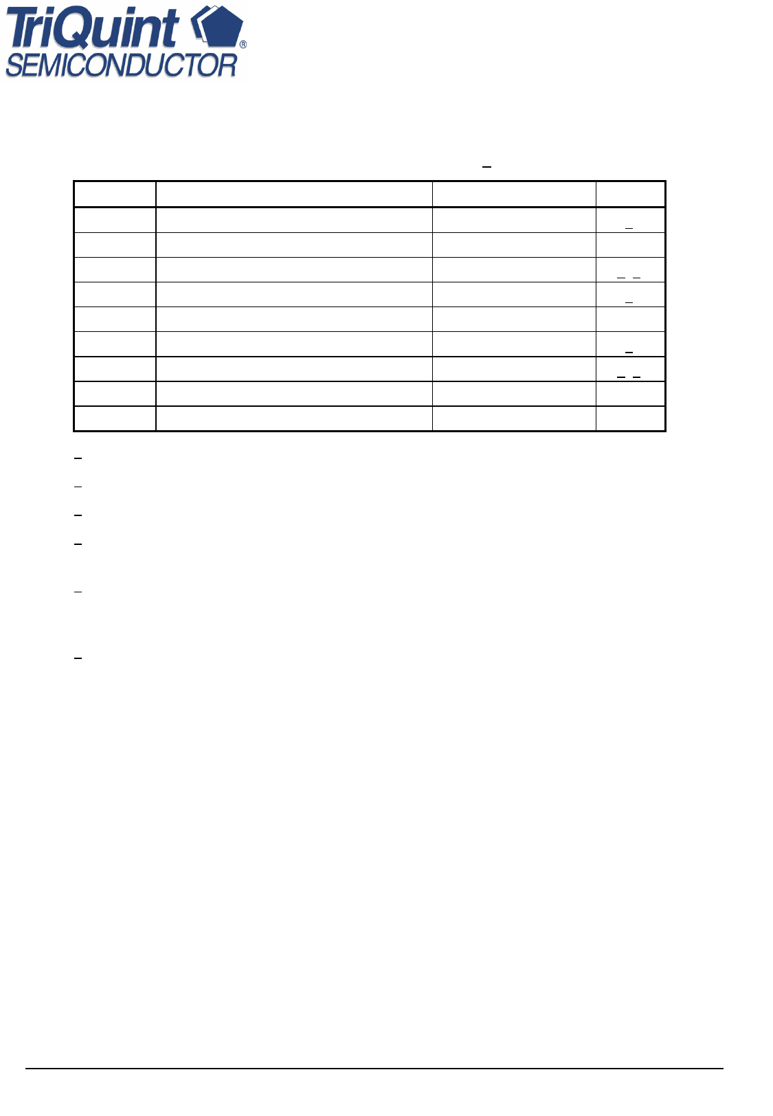
TABLE I
MAXIMUM RATINGS 1/
SYMBOL
PARAMETER
VALUE
NOTES
Vd
Vg
Id
⏐Ig⏐
PIN
PD
TCH
TSTG
Drain Voltage
Gate Voltage Range
Drain Current
Gate Current
Input Continuous Wave Power
Power Dissipation
Operating Channel Temperature
Mounting Temperature (30 Seconds)
Storage Temperature
8V
2/
-2 TO 0 V
700 mA
2/ 3/
16 mA
3/
23 dBm
4.2 W
2/
200 °C
5/ 6/
320 °C
-65 to 150 °C
1/ These ratings represent the maximum operable values for this device.
2/ Combinations of supply voltage, supply current, input power, and output power shall not exceed PD.
3/ Total current for the entire MMIC.
4/ When operated at this bias condition (with RF applied) at a base plate temperature of 70 °C, the
median life is 7.3E+3 hrs.
5/ Junction operating temperature will directly affect the device median time to failure (Tm). For
maximum life, it is recommended that junction temperatures be maintained at the lowest possible
levels.
6/ These ratings apply to each individual FET.
2
TriQuint Semiconductor: www. triquint.com (972)994-8465 Fax (972)994-8504 Info-mmw@tqs.com
May 2009 © Rev -
Share Link: 