8XL196NP データシートの表示(PDF) - Intel
部品番号
コンポーネント説明
メーカー
8XL196NP Datasheet PDF : 34 Pages
| |||
8XL196NP COMMERCIAL CHMOS 16-BIT MICROCONTROLLER
5.0 ELECTRICAL CHARACTERISTICS
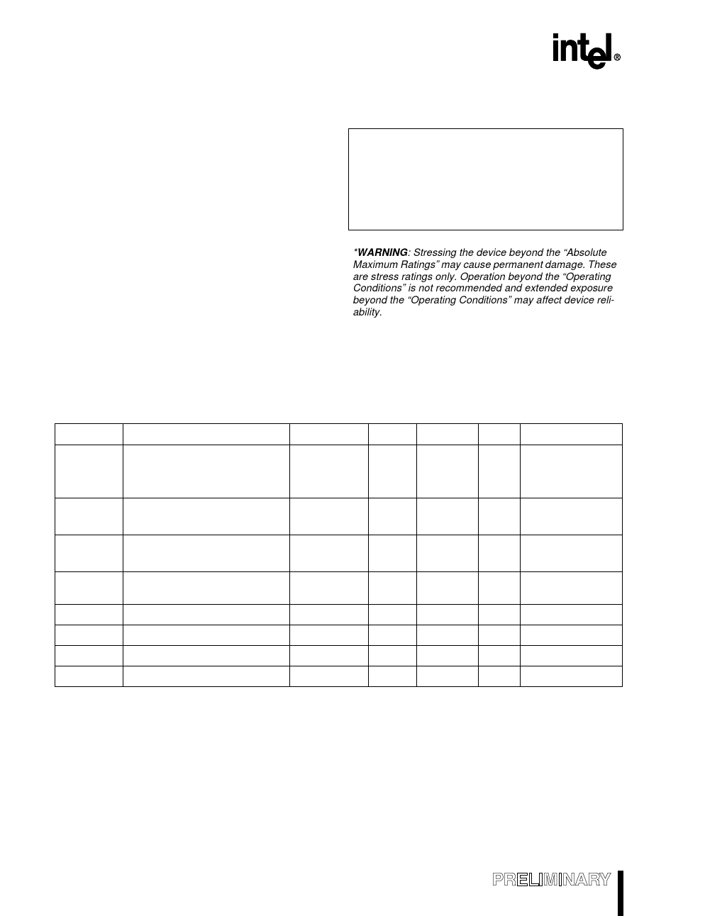
ABSOLUTE MAXIMUM RATINGS*
Storage Temperature ................................. –60°C to +150°C
Supply Voltage with Respect to VSS............. –0.5 V to +7.0 V
Power Dissipation ........................................................ 1.5 W
OPERATING CONDITIONS*
TA (Ambient Temperature Under Bias) ..............0°C to +70°C
VCC (Digital Supply Voltage) ............................ 2.7 V to 3.3 V
FXTAL1 (Input Frequency for VCC = 2.7–3.3 V)
(Note 1).............. 8 MHz to 14 MHz
NOTES:
1. This device is static and should operate below 1 Hz, but
has been tested only down to 8 MHz.
NOTICE: This document contains information on
products in the design phase of development. The
specifications are subject to change without notice.
Do not finalize a design with this information.
Revised information will be published when the
product is available. Verify with your local Intel
sales office that you have the latest datasheet
before finalizing a design.
*WARNING: Stressing the device beyond the “Absolute
Maximum Ratings” may cause permanent damage. These
are stress ratings only. Operation beyond the “Operating
Conditions” is not recommended and extended exposure
beyond the “Operating Conditions” may affect device reli-
ability.
5.1 DC Characteristics
Symbol
ICC
IIDLE
IPD
Table 8. DC Characteristics at VCC = 2.7 – 3.3 V
Parameter
Min
Typ(1)
Max
VCC Supply Current
28
40
Idle Mode Current
Powerdown Mode Current
(Note 2)
14
25
50
75
Units Test Conditions
mA XTAL1 = 14MHz
VCC = 3.3V
Device in Reset
mA XTAL1 = 14MHz
VCC = 3.3 V
µA VCC = 3.3V
ILI
Input Leakage Current
(all input pins except RESET)
±10
µA VSS < VIN < VCC
VIL
Input Low Voltage (all pins)
–0.5
0.4
V
VIH
Input High Voltage
0.2 VCC +1.3
VCC + 0.5 V
VIL1
Input Low Voltage XTAL1
–0.5
0.3 VCC
V
VIH1
Input High Voltage XTAL1
0.7 VCC
VCC + 0.5 V
NOTES:
1. Typical values are based on a limited number of samples and are not guaranteed. The values listed
are at room temperature and with VCC = 3.0 V.
2. For temperatures below 100°C, typical is 10 µA.
3. For all pins except P4.3:0, which have higher drive capability.
4. If VOL is held above 0.45 V or VOH is held below Vcc–0.7 V, current on pins must be externally limited to
the following values: IOL and IOH maximum on all output pins is 12 mA.
5. For all pins that were weakly pulled high during RESET. This excludes ALE, INST, and NMI, which
were weakly pulled low (see VOL2) and ONCE, which was pulled medium low (see VOL3).
6. Pin capacitance is not tested. CS is based on design simulations.
18
Share Link: 