AD10265 データシートの表示(PDF) - Analog Devices
部品番号
コンポーネント説明
メーカー
AD10265
Analog Devices

AD10265 Datasheet PDF : 24 Pages
| |||
AD10265
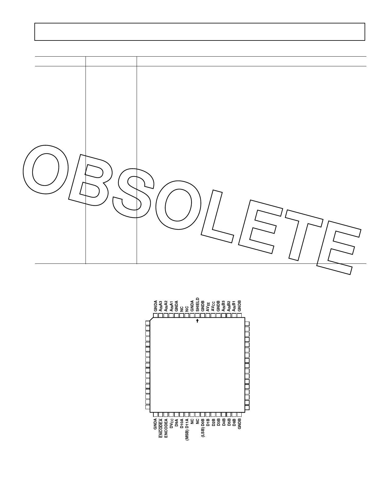
PIN FUNCTION DESCRIPTIONS
Pin No.
Name
Function
1
SHIELD
Internal Ground Shield between channels.
2, 5, 9–11, 26, 27
GNDA
A Channel Ground. A and B grounds should be connected as close to the device as possible.
3, 4, 12, 15, 16,
NC
No Connect. Pins 15 and 16 are internal test pins: it is recommended to connect
34, 35, 55–57
them to GND.
6
AINA1
Analog Input for A side ADC (nominally ± 0.5 V).
7
AINA2
Analog Input for A side ADC (nominally ± 1.0 V).
8
AINA3
Analog Input for A side ADC (nominally ± 2.0 V).
13
AVEE
Analog Negative Supply Voltage (nominally –5.0 V). For A side ADC.
14
AVCC
Analog Positive Supply Voltage (nominally +5.0 V). For A side ADC.
OBSOLETE 17–25,31–33
28
29
30
36–42, 45–49
43, 44, 53, 54,
58–61, 65, 68
50
51
52
62
63
64
66
67
D0A–D11A
ENCODEA
ENCODEA
DVCC
D0B–D11B
GNDB
DVCC
ENCODEB
ENCODEB
AINB1
AINB2
AINB3
AVCC
AVEE
Digital Outputs for ADC A. D0 (LSB).
ENCODE is complement of ENCODE.
Data conversion initiated on rising edge of ENCODE input.
Digital positive supply voltage (nominally 3.3 V) for A side ADC.
Digital Outputs for ADC B. D0 (LSB).
B Channel Ground. A and B grounds should be connected as close to the device
as possible.
Digital Positive Supply Voltage (nominally 3.3 V) for B side ADC.
Data conversion initiated on rising edge of ENCODE input.
ENCODE is complement of ENCODE.
Analog Input for B side ADC (nominally ± 0.5 V).
Analog Input for B side ADC (nominally ± 1.0 V).
Analog Input for B side ADC (nominally ± 2.0 V).
Analog Positive Supply Voltage (nominally +5.0 V). For B side ADC.
Analog Negative Supply Voltage (nominally –5.0 V). For B side ADC.
PIN CONFIGURATION
68-Lead Ceramic Leaded Chip Carrier
9 8 7 6 5 4 3 2 1 68 67 66 65 64 63 62 61
GNDA 10
GNDA 11
NC 12
AVEE 13
AVCC 14
NC 15
NC 16
(LSB) D0A 17
D1A 18
D2A 19
D3A 20
D4A 21
D5A 22
D6A 23
D7A 24
D8A 25
GNDA 26
PIN 1
AD10265
TOP VIEW
(Not to Scale)
60 GNDB
59 GNDB
58 GNDB
57 NC
56 NC
55 NC
54 GNDB
53 GNDB
52 ENCODEB
51 ENCODEB
50 DVCC
49 D11B (MSB)
48 D10B
47 D9B
46 D8B
45 D7B
44 GNDB
27 28 29 30 31 32 33 34 35 36 37 38 39 40 41 42 43
NC = NO CONNECT
REV. A
–5–
Share Link: