STR-A6100 データシートの表示(PDF) - Sanken Electric co.,ltd.
部品番号
コンポーネント説明
メーカー
STR-A6100 Datasheet PDF : 26 Pages
| |||
STR-A6100 Series
9. Operational Description
All of the parameter values used in these descriptions
are typical values of STR-A6151, unless they are
specified as minimum or maximum.
With regard to current direction, "+" indicates sink
current (toward the IC) and "–" indicates source
current (from the IC).
9.1 Startup Operation
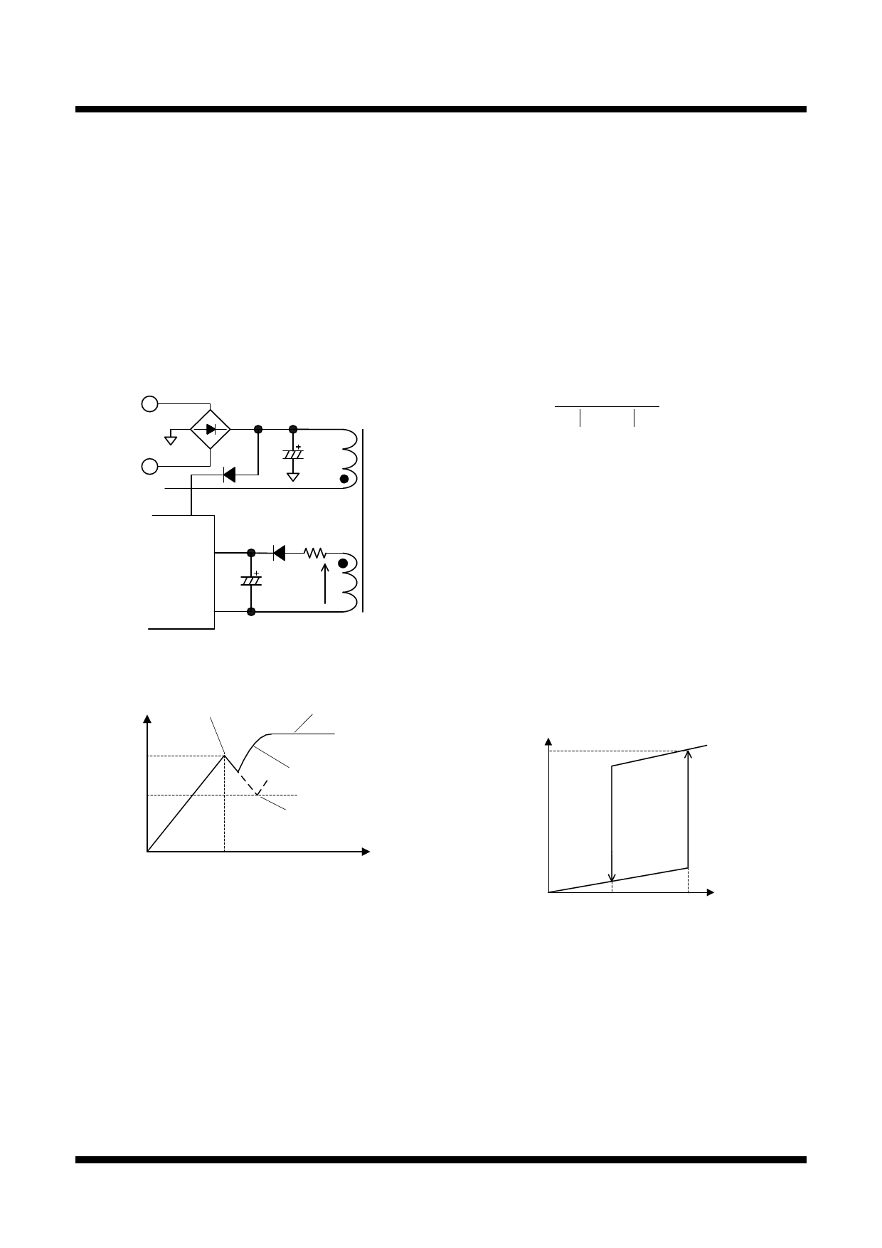
Figure 9-1 shows the circuit around VCC pin. Figure
9-2 shows VCC pin voltage behavior during the startup
period.
VAC
BR1
DST
T1
C1 P
5
U1 ST
VCC 2
3
GND
D2 R2
C2 VD
D
Figure 9-1 VCC pin peripheral circuit
VCC pin voltage IC starts operation Startup success
VCC(ON)
VCC(OFF)
Target operating
voltage
Increase with rising of
output voltage
Startup failure
Time
Figure 9-2 VCC pin voltage during startup period
The IC incorporates the startup circuit. The circuit is
connected to ST pin. During the startup process, the
constant current, ISTARTUP = − 790 µA, charges C2 at
VCC pin. When VCC pin voltage increases to
VCC(ON) = 17.5 V, the IC starts the operation. Then
circuit current increases and VCC pin voltage decreases.
Since the Operation Stop Voltage VCC(OFF) = 10 V is low,
the auxiliary winding voltage reaches to setting value
before VCC pin voltage decreases to VCC(OFF). Thus
control circuit continues the operation. The voltage from
the auxiliary winding D in Figure 9-1 becomes a power
source to the control circuit in operation.
The approximate value of auxiliary winding voltage is
about 15 V to 20 V, taking account of the winding turns
of D winding so that VCC pin voltage becomes
Equation (2) within the specification of input and output
voltage variation of power supply.
VCC(BIAS) (max .) VCC VCC(OVP ) (min.)
⇒11.6(V) VCC 28.7(V)
(1)
The startup time of IC is determined by C2 capacitor
value. The approximate startup time tSTART is
calculated as follows:
t START
C2 ×
VCC(ON )-VCC(INT)
ISTRATUP
(2)
where,
tSTART
VCC(INT)
: Startup time of IC (s)
: Initial voltage on VCC pin (V)
9.2 Undervoltage Lockout (UVLO)
Figure 9-3 shows the relationship of VCC pin voltage
and circuit current ICC. When VCC pin voltage
increases to VCC(ON) = 17.5 V, the control circuit starts
switching operation and the circuit current ICC increases.
When VCC pin voltage decreases to VCC(OFF) = 10 V, the
control circuit stops operation by UVLO (Undervoltage
Lockout) circuit, and reverts to the state before startup.
Circuit current, ICC
ICC(ON)
Stop
Start
VCC(OFF)
VCC(ON)
VCC pin
voltage
Figure 9-3 Relationship between
VCC pin voltage and ICC
9.3 Constant Output Voltage Control
Figure 9-4 shows FB/OLP pin peripheral circuit,
Figure 9-5 shows the waveform of ID and FB
comparator input.
The IC achieves the constant voltage control of the
power supply output by PRC (Pulse Ratio Control). PRC
STR-A6100 - DS Rev.2.1
SANKEN ELECTRIC CO.,LTD.
14
Jun. 05, 2014
Share Link: 