STR-A6100 データシートの表示(PDF) - Sanken Electric co.,ltd.
部品番号
コンポーネント説明
メーカー
STR-A6100 Datasheet PDF : 26 Pages
| |||
STR-A6100 Series
consumption because the switching period in this
intermittent operation is short compared with oscillation
stop period. When the abnormal condition is removed,
the IC returns to normal operation automatically.
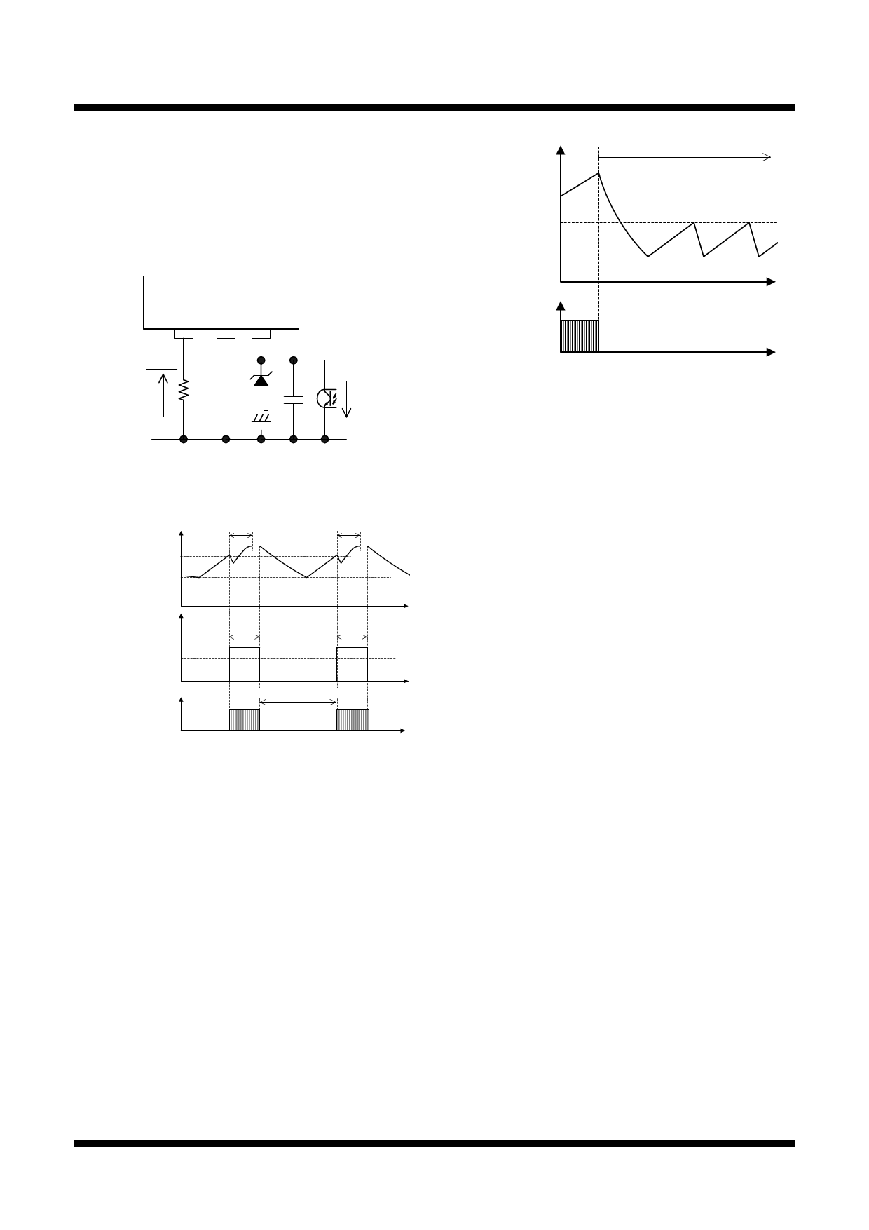
As shown in Figure 9-9, tDLY should be longer than
tSTART which is the period until the output voltage
becomes constant. If tDLY is shorter than tSTART, the
power supply may not start due to OLP operation.
U1
S/OCP GND FB/OLP
1
34
DZ1
VROCP
ROCP
C4
PC1
IFB
C3
Figure 9-8 FB/OLP pin peripheral circuit
VCC pin voltage
VCC(ON)
VCC(OFF)
FB/OLP pin voltage
VOLP
Drain current,
ID
tSTART
tSTART
tDLY
tDLY
Non-switching interval
Figure 9-9 OLP operational waveforms
9.9 Overvoltage Protection (OVP)
Figure 9-10 shows the OVP operational waveforms.
When a voltage between VCC pin and GND terminal
increases to VCC(OVP) = 31.2 V or more, OVP function is
activated. When the OVP function is activated, the IC
stops switching operation at the latched state.
After that, VCC pin voltage is decreased by circuit
current of IC. When VCC pin voltage becomes
VCC(OFF) = 10 V or less, VCC pin voltage is increased by
Startup Current. When VCC pin voltage increases to
VCC(ON) = 17.5 V, the circuit current increases and VCC
pin voltage decreases. In this way, VCC pin voltage
goes up and down between VCC(OFF) and VCC(ON) during
the latched state, excessive increase of VCC pin voltage
is prevented.
Releasing the latched state is done by turning off the
input voltage and by dropping the VCC pin voltage
below VCC(La.OFF) = 7.3 V.
VCC pin voltage
VCC(OVP)=31.2V
VCC(ON)=17.5V
VCC(OFF)=10V
Latched state
Drain current,
ID
Figure 9-10 OVP operational waveforms
If output voltage detection circuit becomes open, the
output voltage of secondary side increases. In case the
VCC pin voltage is provided by using auxiliary winding
of transformer, the overvoltage conditions can be
detected because the VCC pin voltage is proportional to
output voltage. The approximate value of output voltage
VOUT(OVP) in OVP condition is calculated by using
Equation (4).
VOUT(OVP)
VOUT (NORMAL )
VCC(NORMAL )
× 31.2
(4)
where,
VOUT(NORMAL): Output voltage in normal operation
VCC(NORMAL): VCC pin voltage in normal operation
9.10 Thermal Shutdown Function (TSD)
When the temperature of control circuit increases to
Tj(TSD) = 135 °C or more, Thermal Shutdown function
is activated. When the TSD function is activated, the IC
stops switching operation at the latched state (see the
Section 9.9). Releasing the latched state is done by
turning off the input voltage and by dropping the VCC
pin voltage below VCC(La.OFF) = 7.3 V.
STR-A6100 - DS Rev.2.1
SANKEN ELECTRIC CO.,LTD.
17
Jun. 05, 2014
Share Link: 