M50LPW041N データシートの表示(PDF) - STMicroelectronics
部品番号
コンポーネント説明
メーカー
M50LPW041N Datasheet PDF : 37 Pages
| |||
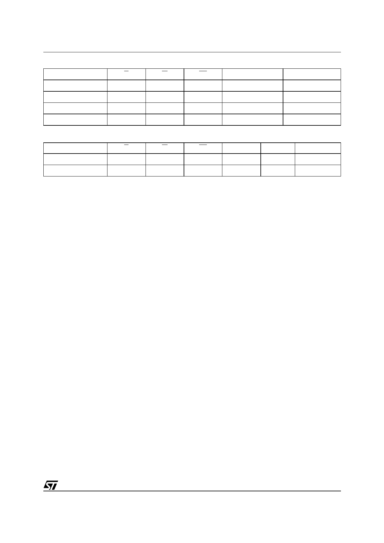
Table 9. A/A Mux Bus Operations
Operation
G
Bus Read
VIL
Bus Write
VIH
Output Disable
VIH
Reset
VIL or VIH
W
VIH
VIL
VIH
VIL or VIH
Table 10. Manufacturer and Device Codes
Operation
G
W
Manufacturer Code
VIL
VIH
Device Code
VIL
VIH
M50LPW041
RP
VPP
DQ7-DQ0
VIH
Don’t Care
Data Output
VIH
Float or VCC or VPPH
Data Input
VIH
Don’t Care
Hi-Z
VIL
Don’t Care
Hi-Z
RP
A18-A1
A0
DQ7-DQ0
VIH
VIL
VIL
20h
VIH
VIL
VIH
3Ch
Register for details on the definitions of the Status
Register bits.
If the address falls in a protected block then the
Program operation will abort, the data in the
memory array will not be changed and the Status
Register will output the error.
During the Program operation the memory will
only accept the Read Status Register command
and the Program/Erase Suspend command. All
other commands will be ignored. Typical Program
times are given in Table 13.
Note that the Program command cannot change a
bit set at ‘0’ back to ‘1’ and attempting to do so will
not cause any modification on its value. One of the
Erase commands must be used to set all of the
bits in the block to ‘1’.
See Figure 14, Program Flowchart and Pseudo
Code, for a suggested flowchart on using the
Program command.
Quadruple Byte Program Command. The Qua-
druple Byte Program Command can be only used
in A/A Mux mode to program four adjacent bytes
in the memory array at a time. The four bytes must
differ only for the addresses A0 and A1.
Programming should not be attempted when VPP
is not at VPPH. The operation can also be executed
if VPP is below VPPH, but result could be uncertain.
Five Bus Write operations are required to issue the
command. The second, the third and the fourth
Bus Write cycle latches respectively the address
and data of the first, the second and the third byte
in the internal state machine. The fifth Bus Write
cycle latches the address and data of the fourth
byte in the internal state machine and starts the
Program/Erase Controller. Once the command is
issued subsequent Bus Read operations read the
Status Register. See the section on the Status
Register for details on the definitions of the Status
Register bits.
During the Quadruple Byte Program operation the
memory will only accept the Read Status register
command and the Program/Erase Suspend com-
mand. All other commands will be ignored. Typical
Quadruple Byte Program times are given in Table
13.
Note that the Quadruple Byte Program command
cannot change a bit set to ‘0’ back to ‘1’ and
attempting to do so will not cause any modification
on its value. One of the Erase commands must be
used to set all of the bits in the block to ‘1’.
See Figure 15, Quadruple Byte Program Flow-
chart and Pseudo Code, for a suggested flowchart
on using the Quadruple Byte Program command.
Chip Erase Command. The Chip Erase Com-
mand can be only used in A/A Mux mode to erase
the entire chip at a time. Erasing should not be at-
tempted when VPP is not at VPPH. The operation
can also be executed if VPP is below VPPH, but re-
sult could be uncertain. Two Bus Write operations
are required to issue the command and start the
Program/Erase Controller. Once the command is
issued subsequent Bus Read operations read the
Status Register. See the section on the Status
Register for details on the definitions of the Status
Register bits. During the Chip Erase operation the
memory will only accept the Read Status Register
command. All other commands will be ignored.
Typical Chip Erase times are given in Table 13.
The Chip Erase command sets all of the bits in the
memory to ‘1’. See Figure 17, Chip Erase Flow-
chart and Pseudo Code, for a suggested flowchart
on using the Chip Erase command.
11/37
Share Link: 