CXB1818Q データシートの表示(PDF) - Sony Semiconductor
部品番号
コンポーネント説明
メーカー
CXB1818Q Datasheet PDF : 17 Pages
| |||
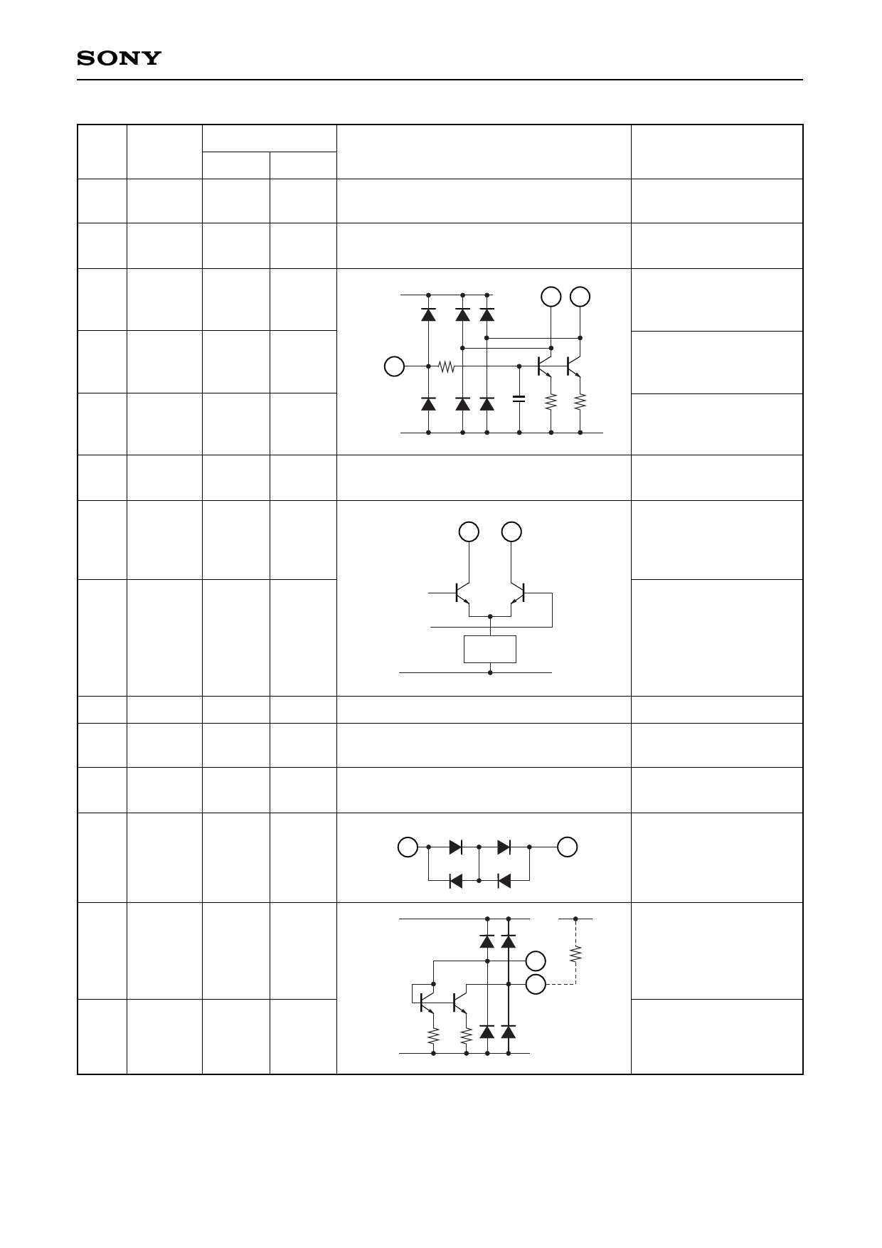
Pin Description
Pin
No.
Typical pin voltage [V]
Symbol
DC
AC
1 VCC4
3.3
2 VEE4
0
3 BiasAdj 1.5 to 0
4 SBias
5 Bias
0mA
to
2.5mA
0mA
to
60mA
6 VEE5
0
7Q
6mA
to 30mA∗1
1.3 to 3.3 6mA
to 50mA∗2
9 QBX
6mA
to 30mA∗1
1.3 to 3.3 6mA
to 50mA∗2
8 NC
10 VEE1
—
—
0
11 VCC1
3.3
12 TM
1.5
Equivalent circuit
VCC
45
260
3
30
10pF
240
8
VEE
7
9
Current
Source
VEE
VEE
12
10
CXB1818Q
Description
Positive power supply
for APC circuit.
Negative power supply
for APC circuit.
Bias current setting.
Bias current setting or
monitor.
Bias current output.
Open collector output.
Negative power supply
for bias circuit.
Modulation current
output.
Open collector output.
Complementary current
output.
Q and QBX are not
symmetrical output.
Use Q output for laser
diode.
No connected.
Negative power supply
for driver circuit.
Positive power supply
for driver circuit.
Chip temperature
monitor.
13 DrvMon
0mA
to
1.4mA
14 DrvAdj
0mA
to
9mA
∗1 Ta = –40 to 0°C
∗2 Ta = 0 to +85°C
VCC
22.5 150
VEE
–3–
Modulation current (IQ)
Rmon monitor.
IQ is monitored by
14
connecting a resistor
13
(Rmon) to this pin.
Modulation current (IQ)
setting.
Share Link: 