CXB1818Q データシートの表示(PDF) - Sony Semiconductor
部品番号
コンポーネント説明
メーカー
CXB1818Q Datasheet PDF : 17 Pages
| |||
CXB1818Q
Pin
No.
Typical pin voltage [V]
Symbol
DC
AC
29 SDNB
VCC
0 to 3.3
30 SDN
29
30
0 to 3.3
VEE
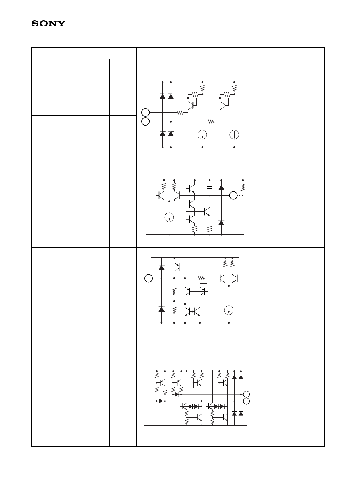
Equivalent circuit
Description
5k 5k
5k 5k
Complementary TTL
300
input to disable the
300
output current.
(Shutdown input)
60µA
When left open, High.
60µA
31 Tset
32 VREF
1.7
33 VCC6
3.3
VCC
2.4k
2.4k 20pF
70µA
VEE
220 140
Output duty cycle
control.
Rset
This pin controls the
31
falling edge of the input
High pulse. Variable
delay limit of that is from
0 to 1.0ns. Duty cycle is
controlled by connecting
a resistor value between
VCC and this pin.
VCC
32
2.4k
9.1k
VEE
300
200
300
1.9mA
Temperature
compensated reference
voltage for APC.
Approximately 1.7V
(Constant for VEE
reference)
Positive power supply
for alarm output circuit.
34 LDAlm
VCC
0.2 to 3.0
35 LDAlmB
0.2 to 3.0 VEE
Activates when the
fault is detected in the
34 laser monitor diode
35 circuit.
(Pseudo LVTTL output)
–6–
Share Link: 