TH8060JDF データシートの表示(PDF) - Melexis Microelectronic Systems
部品番号
コンポーネント説明
メーカー
TH8060JDF Datasheet PDF : 16 Pages
| |||
TH8060
LIN Bus Transceiver with integrated Voltage Regulator
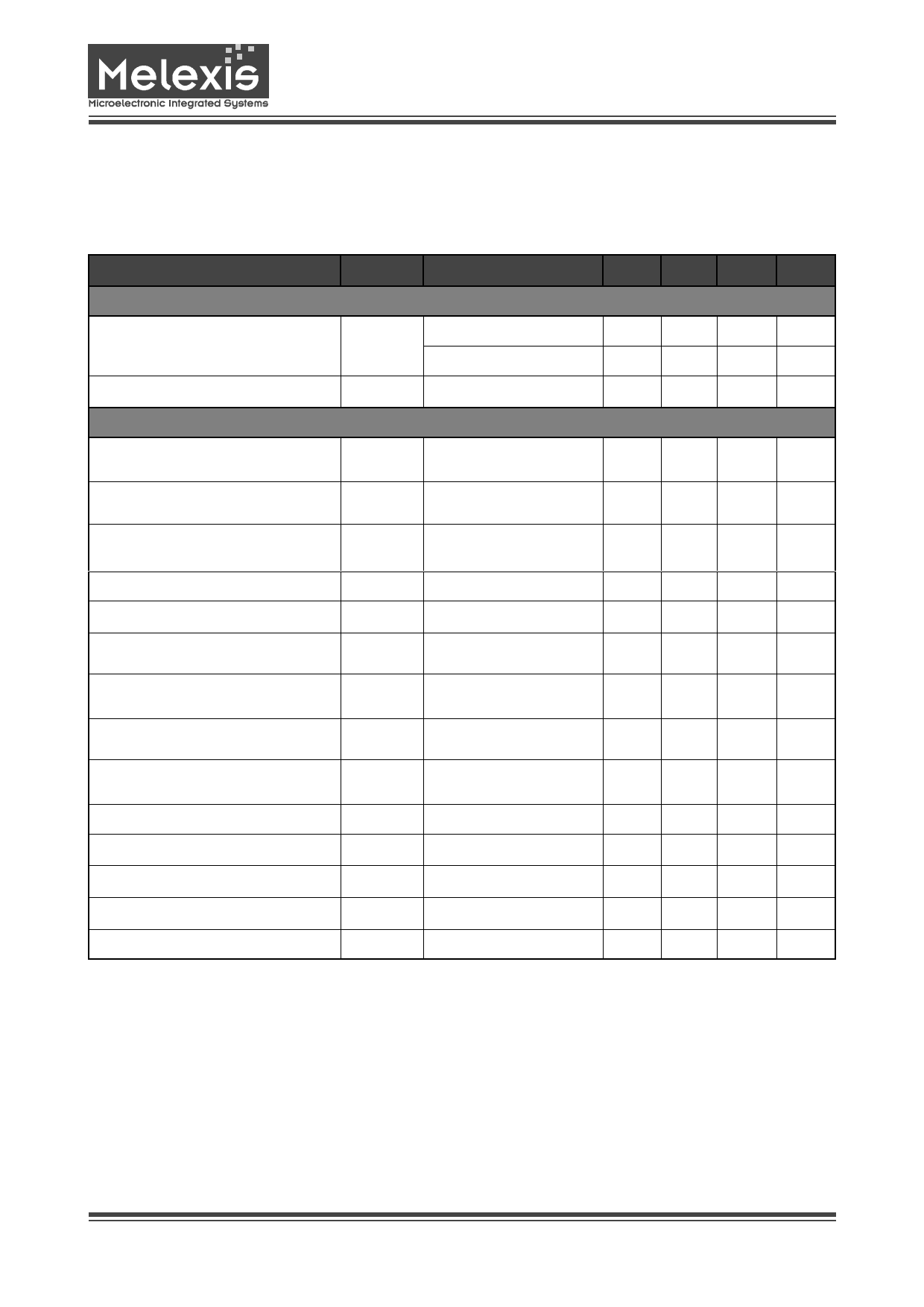
Dynamic Characteristics
All dynamic values of the table below refer to the test-schematic schown in Figure 3 - Test Circuit for Dynamic
Characteristics
For the definition of delay and transitions times see Figure 2 - TH8060 Timing Diagram.
(7V ≤ VSUP ≤ 18V, 4.75V ≤ VCC ≤ 5.25V, -40°C ≤ TA ≤ 125°C, unless otherwise specified)
Parameter
Symbol Condition
Min Typ Max Unit
RESET
Reset time
Reset rising time
tRes
RVTR < 1 kΩ
RVTR > 45 kΩ
trr
70
100
140
ms
10
15
20
ms
3.0
6.5
10
µs
LIN-Bus-Interface
Slew rate BUS falling edge [2]
Slew rate BUS rising edge [2]
Symmetry of Slew rate BUS
Debouncing time BUS
Symmetry of debouncing BUS
Propagation delay TxD -> BUS [1] [2]
Symmetry of propagation delay
TxD -> BUS [1]
Propagation delay BUS -> RxD [1] [2]
Symmetry of propagation delay
BUS -> RxD [1]
Debouncing time TxD [1]
Debouncing time EN [1]
Wake-up-debouncing BUS
Propagation delay SI -> SO
VSUP-SENSE debouncing [1]
dV/dTfall
dV/dTrise
dV/dTsym
tdebBUS
tdebsym
ttrans_pdr,
ttrans_pdf
20% ≤ VBUS ≤ 80%
100pF ≤ CBUS ≤ 10nF
20% ≤ VBUS ≤ 80%
CBUS = 100 pF
dV/dTrise - dV/dTfall
CBUS = 100 pF
High pulse or low pulse
ttrans_sym
trec_pdr
ttrec_pdf
ttrans_pdr - ttrans_pdf
trec_sym
trec_pdr - trec_pdf
tdeb
tdeb
tdebWake
tpdcomp
tdeb
-2.5 -2.0 -1.0 V/µs
1.0
2.0
2.5 V/µs
-0.3
1.5
2.8
-0.5
-2
-2
0.6
1.0
200
25
45
4
10
17
0.3 V/µs
4.0
µs
0.5
µs
4
µs
2
µs
6
µs
2
µs
1.5
µs
ns
90
µs
11
µs
25
µs
______________________________
[1] See timing diagram
[2] See test circuit for dynamic characteristics on page 12
Datasheet Rev 1.1 March 2001
Page 11
www.melexis.com
Share Link: 