87C196LA データシートの表示(PDF) - Intel
部品番号
コンポーネント説明
メーカー
87C196LA Datasheet PDF : 21 Pages
| |||
87C196LA — AUTOMOTIVE
3.0 SIGNALS
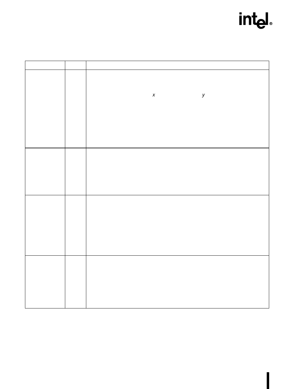
Name
ACH7:2
AD15:0
ADV#
AINC#
Type
I
I/O
O
I
Table 4. Signal Descriptions
Description
Analog Channels
These signals are analog inputs to the A/D converter.
The A/D inputs share package pins with port 0. These pins may individually be
used as analog inputs (ACHx) or digital inputs (P0.y). While it is possible for the
pins to function simultaneously as analog and digital inputs, this is not
recommended because reading port 0 while a conversion is in process can
produce unreliable conversion results.
The ANGND and VREF pins must be connected for the A/D converter and port 0
to function.
ACH7:2 share package pins with the following signals: ACH2/P0.2, ACH3/P0.3,
ACH4/P0.4/PMODE.0, ACH5/P0.5/PMODE.1, ACH6/P0.6/PMODE.2, and
ACH7/P0.7/PMODE.3.
Address/Data Lines
These pins provide a multiplexed address and data bus. During the address
phase of the bus cycle, address bits 0–15 are presented on the bus and can be
latched using ALE or ADV#. During the data phase, 8- or 16-bit data is
transferred.
AD7:0 share package pins with P3.7:0 and PBUS.7:0; AD15:8 share package
pins with P4.7:0 and PBUS.15:8.
Address Valid
This active-low output signal is asserted only during external memory
accesses. ADV# indicates that valid address information is available on the
system address/data bus. The signal remains low while a valid bus cycle is in
progress and is returned high as soon as the bus cycle completes.
An external latch can use this signal to demultiplex the address from the
address/data bus. A decoder can also use this signal to generate chip selects
for external memory.
ADV# shares a package pin with P5.0 and ALE.
Auto Increment
During slave programming, this active-low input enables the auto-increment
feature. (Auto increment allows reading or writing of sequential OTPROM
locations, without requiring address transactions across the programming bus
for each read or write.) AINC# is sampled after each location is programmed or
dumped. If AINC# is asserted, the address is incremented and the next data
word is programmed or dumped.
AINC# shares a package pin with P2.4.
8
PRODUCT PREVIEW
Share Link: 