SST39VF1601 データシートの表示(PDF) - Silicon Storage Technology
部品番号
コンポーネント説明
メーカー
SST39VF1601 Datasheet PDF : 31 Pages
| |||
16 Mbit / 32 Mbit Multi-Purpose Flash Plus
SST39VF1601 / SST39VF3201
SST39VF1602 / SST39VF3202
Data Sheet
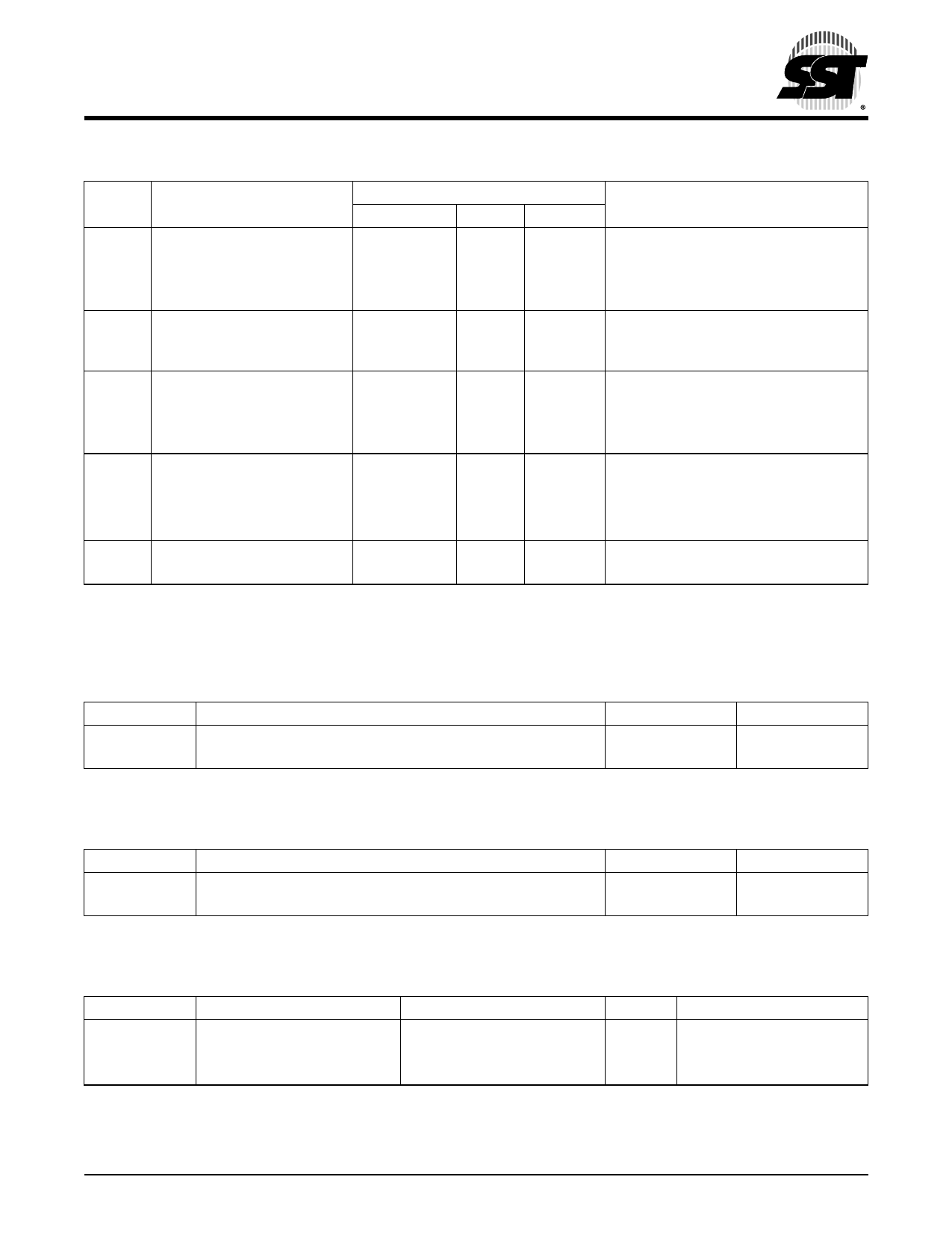
TABLE 11: DC Operating Characteristics VDD = 2.7-3.6V1
Limits
Symbol Parameter
IDD
Power Supply Current
Read3
Program and Erase
ISB
Standby VDD Current
IALP
Auto Low Power
ILI
Input Leakage Current
ILIW
Input Leakage Current
on WP# pin and RST#
Min
Max
Units Test Conditions
Address input=VILT/VIHT2, at f=5 MHz,
VDD=VDD Max
18
mA
CE#=VIL, OE#=WE#=VIH, all I/Os open
35
mA
CE#=WE#=VIL, OE#=VIH
20
µA
CE#=VIHC, VDD=VDD Max
20
µA
CE#=VILC, VDD=VDD Max
All inputs=VSS or VDD, WE#=VIHC
1
µA
VIN=GND to VDD, VDD=VDD Max
10
µA
WP#=GND to VDD or RST#=GND to VDD
ILO
Output Leakage Current
10
µA
VOUT=GND to VDD, VDD=VDD Max
VIL
Input Low Voltage
0.8
V
VDD=VDD Min
VILC
Input Low Voltage (CMOS)
0.3
V
VDD=VDD Max
VIH
Input High Voltage
0.7VDD
V
VDD=VDD Max
VIHC
Input High Voltage (CMOS)
VDD-0.3
V
VDD=VDD Max
VOL
Output Low Voltage
0.2
V
IOL=100 µA, VDD=VDD Min
VOH
Output High Voltage
VDD-0.2
V
IOH=-100 µA, VDD=VDD Min
1. Typical conditions for the Active Current shown on the front page of the data sheet are average values at 25°C
(room temperature), and VDD = 3V. Not 100% tested.
2. See Figure 18
3. The IDD current listed is typically less than 2mA/MHz, with OE# at VIH. Typical VDD is 3V.
T11.8 1223
TABLE 12: Recommended System Power-up Timings
Symbol
Parameter
Minimum
Units
TPU-READ1
Power-up to Read Operation
100
µs
TPU-WRITE1
Power-up to Program/Erase Operation
100
µs
T12.0 1223
1. This parameter is measured only for initial qualification and after a design or process change that could affect this parameter.
TABLE 13: Capacitance (TA = 25°C, f=1 Mhz, other pins open)
Parameter
Description
Test Condition
Maximum
CI/O1
CIN1
I/O Pin Capacitance
Input Capacitance
VI/O = 0V
VIN = 0V
12 pF
6 pF
T13.0 1223
1. This parameter is measured only for initial qualification and after a design or process change that could affect this parameter.
TABLE 14: Reliability Characteristics
Symbol
Parameter
Minimum Specification
Units
Test Method
NEND1,2
Endurance
10,000
Cycles
JEDEC Standard A117
TDR1
ILTH1
Data Retention
Latch Up
100
100 + IDD
Years
mA
JEDEC Standard A103
JEDEC Standard 78
T14.2 1223
1. This parameter is measured only for initial qualification and after a design or process change that could affect this parameter.
2. NEND endurance rating is qualified as a 10,000 cycle minimum for the whole device. A sector- or block-level rating would result in a
higher minimum specification.
©2008 Silicon Storage Technology, Inc.
13
S71223-05-000
6/08
Share Link: 