SST39VF1601 データシートの表示(PDF) - Silicon Storage Technology
部品番号
コンポーネント説明
メーカー
SST39VF1601 Datasheet PDF : 31 Pages
| |||
Data Sheet
16 Mbit / 32 Mbit Multi-Purpose Flash Plus
SST39VF1601 / SST39VF3201
SST39VF1602 / SST39VF3202
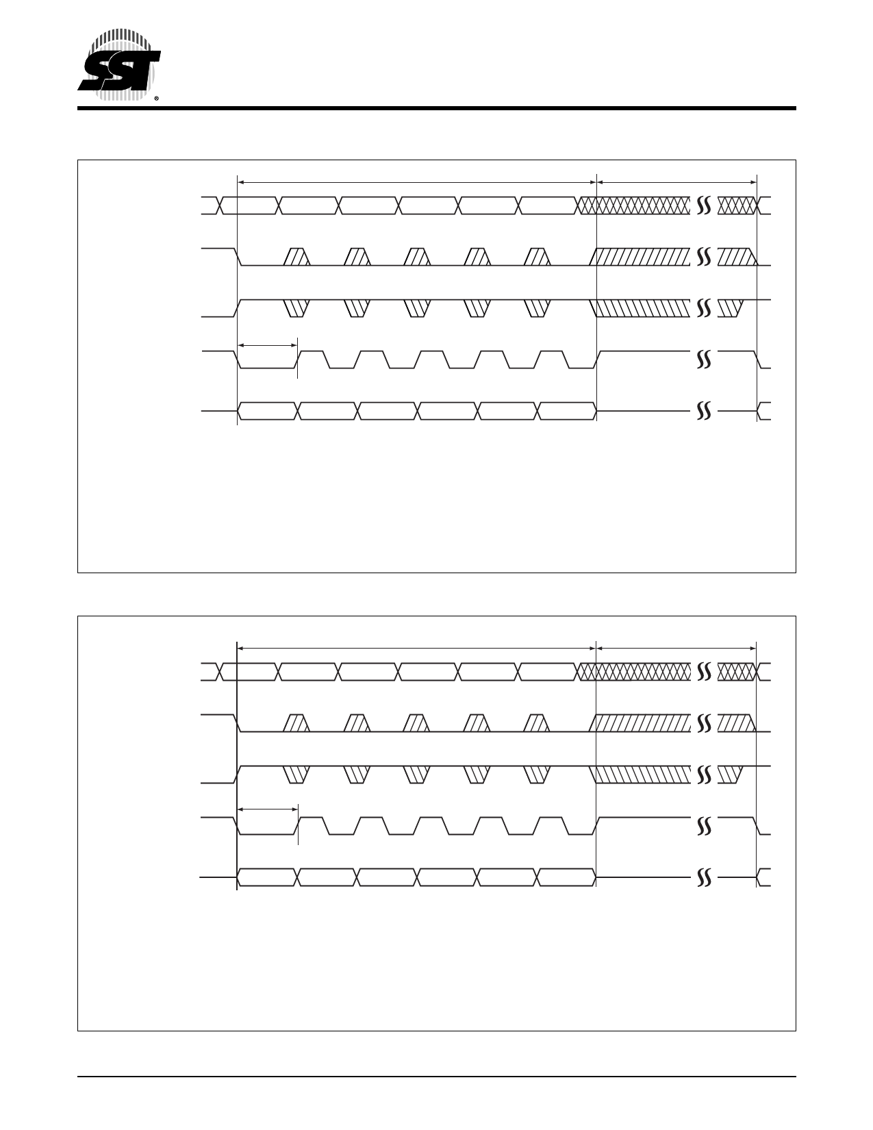
SIX-BYTE CODE FOR BLOCK-ERASE
TBE
ADDRESS AMS-0
5555
2AAA
5555
5555
2AAA
BAX
CE#
OE#
WE#
TWP
DQ15-0
XXAA
SW0
XX55
SW1
XX80
SW2
XXAA
SW3
XX55
SW4
XX50
SW5
Note: This device also supports CE# controlled Block-Erase operation. The WE# and CE# signals are
interchageable as long as minimum timings are met. (See Table 17)
BAX = Block Address
AMS = Most significant address
AMS = A19 for SST39VF1601/1602 and A20 for SST39VF3201/3202
WP# must be held in proper logic state (VIL or VIH) 1 µs prior to and 1 µs after the command sequence
X can be VIL or VIH, but no other value
FIGURE 10: WE# Controlled Block-Erase Timing Diagram
1223 F09.5
SIX-BYTE CODE FOR SECTOR-ERASE
TSE
ADDRESS AMS-0
5555 2AAA
5555
5555
2AAA
SAX
CE#
OE#
WE#
TWP
DQ15-0
XXAA
SW0
XX55
SW1
XX80
SW2
XXAA
SW3
XX55
SW4
XX30
SW5
Note: This device also supports CE# controlled Sector-Erase operation. The WE# and CE# signals are
interchageable as long as minimum timings are met. (See Table 17)
SAX = Sector Address
AMS = Most significant address
AMS = A19 for SST39VF1601/1602 and A20 for SST39VF3201/3202
WP# must be held in proper logic state (VIL or VIH) 1 µs prior to and 1 µs after the command sequence
X can be VIL or VIH, but no other value
FIGURE 11: WE# Controlled Sector-Erase Timing Diagram
1223 F10.5
©2008 Silicon Storage Technology, Inc.
18
S71223-05-000
6/08
Share Link: 