SST39VF1601 データシートの表示(PDF) - Silicon Storage Technology
部品番号
コンポーネント説明
メーカー
SST39VF1601 Datasheet PDF : 31 Pages
| |||
16 Mbit / 32 Mbit Multi-Purpose Flash Plus
SST39VF1601 / SST39VF3201
SST39VF1602 / SST39VF3202
Data Sheet
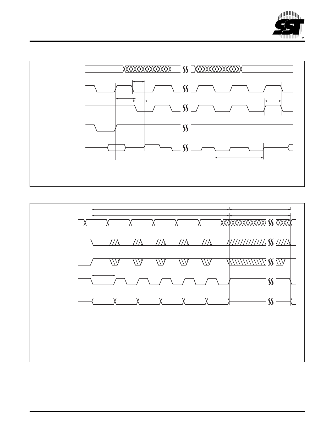
ADDRESS AMS-0
CE#
OE#
TCE
TOEH
TOE
TOES
WE#
DQ6 and DQ2
Note:
AMS = Most significant address
AMS = A19 for SST39VF1601/1602 and A20 for SST39VF3201/3202
TWO READ CYCLES
WITH SAME OUTPUTS
FIGURE 8: Toggle Bits Timing Diagram
1223 F07.4
ADDRESS AMS-0
ADDRESS AMS-0
CE#
CE#
5555
5555
2AAA
2AAA
SIX-BYTE CODE FOR CHIP-ERASE
SIX-BYTE CODE FOR CHIP-ERASE
5555
5555
2AAA
5555
5555
2AAA
5555
5555
TSCE
TSCE
OE#
OE#
WE#
WE#
TWP
TWP
DQ15-0
DQ15-0
XXAA
XXAA
SW0
SW0
XX55
XX55
SW1
SW1
XX80
XX80
SW2
SW2
XXAA
XXAA
SW3
SW3
XX55
XX55
SW4
SW4
XX10
XX10
SW5
SW5
Note:
Note:
This device also supports CE# controlled Chip-Erase operation. The WE# and CE# signals are
iTnhteisrcdheavgiceeaballesoasulopnpgorats CmEin#imcounmtrtoimlleindgCshaipre-Emraest.e(SopeerTaatibolne. 1T7h)e WE# and CE# signals are
AinMteSrc=haMgoesatbsleignaisficloanngt adsdmreinsismum timings are met. (See Table 17)
AMS = AM1o9sftosrigSnSifTic3a9nVt Fa1d6d0re1s/1s602 and A20 for SST39VF3201/3202
WAMPS#=mAu1s9t bfoer hSeSldT3in9VprFo1p6e0r1lo/1g6ic02stanted(AV2IH0)fo1rµSsSpTr3io9rVtoF3a2n0d11/3µ2s02after the command sequence
XWcPa#nmbuesVt IbLeohr eVldIHi,nbpurtonpoerotlohgeircvsatlautee (VIH) 1 µs prior to and 1 µs after the command sequence
X can be VIL or VIH, but no other value
FIGURE 9: WE# Controlled Chip-Erase Timing Diagram
1223 F08.5
1223 F08.5
©2008 Silicon Storage Technology, Inc.
17
S71223-05-000
6/08
Share Link: 