S25FL032P データシートの表示(PDF) - Cypress Semiconductor
部品番号
コンポーネント説明
メーカー
S25FL032P Datasheet PDF : 60 Pages
| |||
S25FL032P
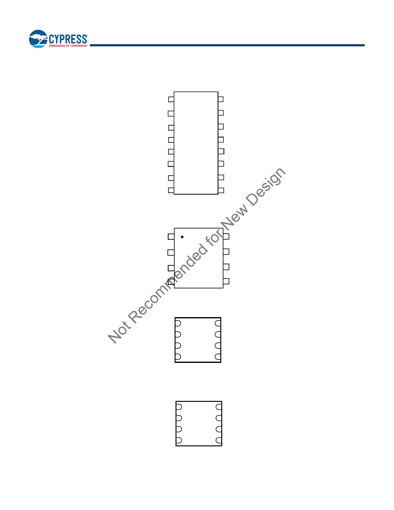
2. Connection Diagrams
Figure 1. 16-pin Plastic Small Outline Package (SO)
HOLD#/IO3 1
16 SCK
VCC 2
15 SI/IO0
DNC 3
14 DNC
DNC 4
DNC 5
13 DNC
12 DNC
DNC 6
11 DNC
Note
DNC = Do Not Connect (Reserved for future use)
CS#
7
SO/IO1
8
10
9
n GND
Desig W#/ACC/IO2
w Figure 2. 8-pin Plastic Small Outline Package (SO)
r Ne CS# 1
fo SO/IO1 2
ded W#/ACC/IO2 3
en GND 4
8 VCC
7 HOLD#/IO3
6 SCK
5 SI/IO0
comm Figure 3. 8-contact USON (5 x 6 mm) Package
Re CS# 1
8
ot SO/IO1 2
7
USON
N W#/ACC/IO2 3
6
VCC
HOLD#/IO3
SCK
GND 4
5 SI/IO0
Note
There is an exposed central pad on the underside of the USON package. This should not be connected to any voltage or signal line on the PCB. Connecting the central
pad to GND (VSS) is possible, provided PCB routing ensures 0mV difference between voltage at the USON GND (VSS) lead and the central exposed pad.
Figure 4. 8-contact WSON Package (6 x 8 mm)
CS#
SO/IO1
W#/ACC/IO2
1
8
2
7
WSON
3
6
VCC
HOLD#/IO3
SCK
GND 4
5 SI/IO0
Note
There is an exposed central pad on the underside of the WSON package. This should not be connected to any voltage or signal line on the PCB. Connecting the central
pad to GND (VSS) is possible, provided PCB routing ensures 0mV difference between voltage at the WSON GND (VSS) lead and the central exposed pad.
Document Number: 002-00650 Rev. *L
Page 5 of 60
Share Link: 