KSZ9031RNX(2012) データシートの表示(PDF) - Micrel
部品番号
コンポーネント説明
メーカー
KSZ9031RNX Datasheet PDF : 75 Pages
| |||
Micrel, Inc.
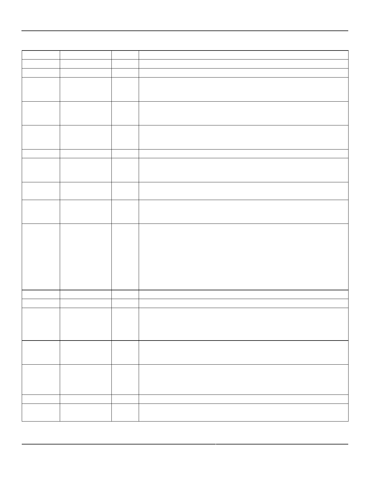
Pin Number
17
Pin Name
LED1/
PHYAD0/
PME_N1
18
DVDDL
19
TXD0
20
TXD1
21
TXD2
22
TXD3
23
DVDDL
24
GTX_CLK
25
TX_EN
26
DVDDL
27
RXD3/
MODE3
28
RXD2/
MODE2
29
VSS
30
DVDDL
KSZ9031RNX
Type(1)
I/O
Pin Function
LED1 output:
Config mode:
PME_N output:
Programmable LED1 output
The voltage on this pin is sampled and latched during the power-
up/reset process to determine the value of PHYAD[0]. See the
“Strapping Options” section for details.
Programmable PME_N output (pin option 1). This pin function
requires an external pull-up resistor to DVDDH (digital VDD_I/O)
in a range from 1.0kΩ to 4.7kΩ. When asserted low, this pin
signals that a WOL event has occurred.
The LED1 pin is programmed by the LED_MODE strapping option (pin 41), and is
defined as follows.
Single-LED Mode
Activity
Pin State LED Definition
No activity
H
OFF
Activity (RX, TX)
Toggle Blinking
Tri-Color Dual-LED Mode
Link/Activity
Link off
1000 Link / No activity
1000 Link / Activity (RX, TX)
100 Link / No activity
100 Link / Activity (RX, TX)
10 Link / No activity
10 Link / Activity (RX, TX)
Pin State
LED2 LED1
H
H
L
H
Toggle H
H
L
H
Toggle
L
L
Toggle Toggle
LED Definition
LED2 LED1
OFF
OFF
ON
OFF
Blinking OFF
OFF
ON
OFF
Blinking
ON
ON
Blinking Blinking
For tri-color dual-LED mode, LED1 works in conjunction with LED2 (pin 15) to
indicate 10Mbps link and activity.
P
1.2V digital VDD
I
RGMII mode: RGMII TD0 (Transmit Data 0) input
I
RGMII mode: RGMII TD1 (Transmit Data 1) input\
I
RGMII mode: RGMII TD2 (Transmit Data 2) input
I
RGMII mode: RGMII TD3 (Transmit Data 3) input
P
1.2V digital VDD
I
RGMII mode: RGMII TXC (Transmit Reference Clock) input
I
RGMII mode: RGMII TX_CTL (Transmit Control) input
P
1.2V digital VDD
I/O RGMII mode: RGMII RD3 (Receive Data 3) output
Config mode: The pull-up/pull-down value is latched as MODE3 during
power-up/reset. See the “Strapping Options” section for details.
I/O RGMII mode: RGMII RD2 (Receive Data 2) output
Config mode: The pull-up/pull-down value is latched as MODE2 during
power-up/reset. See the “Strapping Options” section for details.
Gnd Digital ground
P
1.2V digital VDD
October 2012
12
M9999-103112-1.0
Share Link: 