74ALVT16543DGG データシートの表示(PDF) - NXP Semiconductors.
部品番号
コンポーネント説明
メーカー
74ALVT16543DGG Datasheet PDF : 16 Pages
| |||
Philips Semiconductors
2.5 V/3.3 V 16-bit registered transceiver (3-State)
Product data sheet
74ALVT16543
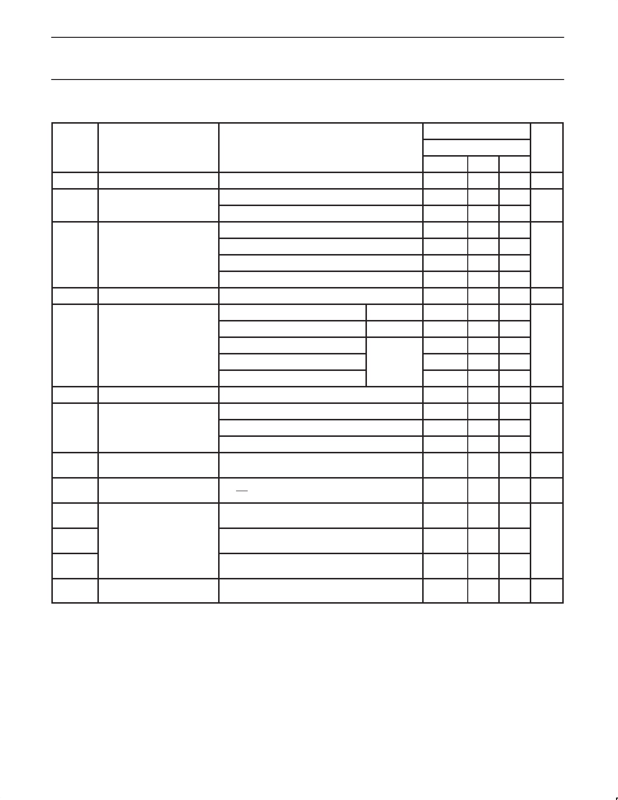
DC ELECTRICAL CHARACTERISTICS (3.3 V ± 0.3 V RANGE)
LIMITS
SYMBOL
PARAMETER
TEST CONDITIONS
Temp = –40 °C to +85 °C
MIN
TYP1 MAX
UNIT
VIK
Input clamp voltage
VCC = 3.0 V; IIK = –18 mA
–
–0.85 –1.2
V
VOH HIGH-level output voltage
VCC = 3.0 V to 3.6 V; IOH = –100 µA
VCC = 3.0 V; IOH = –32 mA
VCC – 0.2 VCC
–
V
2.0
2.3
–
VCC = 3.0 V; IOL = 100 µA
–
0.07 0.2
VOL LOW–level output voltage
VCC = 3.0 V; IOL = 16 mA
VCC = 3.0 V; IOL = 32 mA
–
0.25 0.4
V
–
0.3 0.5
VCC = 3.0 V; IOL = 64 mA
–
0.4 0.55
VRST Power-up output low voltage6 VCC = 3.6 V; IO = 1 mA; VI = VCC or GND
–
–
0.55
V
VCC = 3.6 V; VI = VCC or GND
Control pins
–
0.1 ± 1
VCC = 0 V or 3.6 V; VI = 5.5 V
–
0.1
10
II
Input leakage current
VCC = 3.6 V; VI = VCC
VCC = 3.6 V; VI = 0 V
–
0.5
1
µA
Data pins4
–
0.1
–5
VCC = 3.6 V; VI = 5.5 V
–
0.1
20
IOFF
Off current
VCC = 0 V; VI or VO = 0 V to 4.5 V
–
0.1 ± 100 µA
IHOLD
Bus Hold current
Data inputs7
VCC = 3 V; VI = 0.8 V
VCC = 3 V; VI = 2.0 V
VCC = 0 V to 3.6 V; VCC = 3.6 V
75
130
–
–75
–140 –
µA
± 500
–
–
IEX
Current into an output in the
High state when VO > VCC
VO = 5.5 V; VCC = 3.0 V
–
50
125
µA
IPU/PD
Power-up/down 3-State output VCC ≤ 1.2 V; VO = 0.5 V to VCC; VI = GND or VCC;
current3
OE/OE = Don’t care
–
40 ± 100 µA
ICCH
VCC = 3.6 V; Outputs HIGH; VI = GND or VCC;
IO = 0 mA
–
0.07 0.1
ICCL Quiescent supply current
VCC = 3.6 V; Outputs LOW; VI = GND or VCC;
IO = 0 mA
–
3.6
5
mA
ICCZ
VCC = 3.6 V; Outputs disabled;
VI = GND or VCC, IO = 0 mA5
–
0.07 0.1
∆ICC
Additional supply current per
input pin2
VCC = 3 V to 3.6 V; One input at VCC – 0.6 V;
Other inputs at VCC or GND
–
0.04 0.4 mA
NOTES:
1. All typical values are at VCC = 3.3 V and Tamb = 25 °C.
2. This is the increase in supply current for each input at the specified voltage level other than VCC or GND.
3. This parameter is valid for any VCC between 0 V and 1.2 V with a transition time of up to 10 msec. From VCC = 1.2 V to VCC = 3.3 V ± 0.3 V
a transition time of 100 µsec is permitted. This parameter is valid for Tamb = 25 °C only.
4. Unused pins at VCC or GND.
5. ICCZ is measured with outputs pulled up to VCC or pulled down to ground.
6. For valid test results, data must not be loaded into the flip-flops (or latches) after applying power.
7. This is the bus hold overdrive current required to force the input to the opposite logic state.
2004 Sep 14
6
Share Link: 