2N120BND データシートの表示(PDF) - Fairchild Semiconductor
部品番号
コンポーネント説明
メーカー
2N120BND
Fairchild Semiconductor

2N120BND Datasheet PDF : 8 Pages
| |||
HGTP2N120BND, HGT1S2N120BNDS
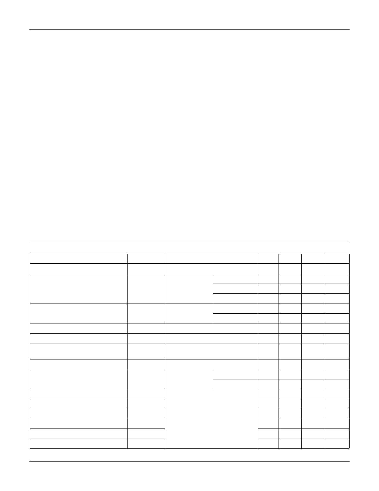
Absolute Maximum Ratings TC = 25oC, Unless Otherwise Specified
Collector to Emitter Voltage . . . . . . . . . . . . . . . . . . . . . . . . . . . . . . . . . . . . . . . . . . . . . BVCES
Collector Current Continuous
At TC = 25oC . . . . . . . . . . . . . . . . . . . . . . . . . . . . . . . . . . . . . . . . . . . . . . . . . . . . . . . . IC25
At TC = 110oC . . . . . . . . . . . . . . . . . . . . . . . . . . . . . . . . . . . . . . . . . . . . . . . . . . . . . . IC110
Collector Current Pulsed (Note 1) . . . . . . . . . . . . . . . . . . . . . . . . . . . . . . . . . . . . . . . . . . .ICM
Gate to Emitter Voltage Continuous. . . . . . . . . . . . . . . . . . . . . . . . . . . . . . . . . . . . . . . . VGES
Gate to Emitter Voltage Pulsed . . . . . . . . . . . . . . . . . . . . . . . . . . . . . . . . . . . . . . . . . . . VGEM
Switching Safe Operating Area at TJ = 150oC (Figure 2) . . . . . . . . . . . . . . . . . . . . . . . SSOA
Power Dissipation Total at TC = 25oC . . . . . . . . . . . . . . . . . . . . . . . . . . . . . . . . . . . . . . . . PD
Power Dissipation Derating TC > 25oC . . . . . . . . . . . . . . . . . . . . . . . . . . . . . . . . . . . . . . . . . .
Operating and Storage Junction Temperature Range . . . . . . . . . . . . . . . . . . . . . . . TJ, TSTG
Maximum Lead Temperature for Soldering
Leads at 0.063in (1.6mm) from case for 10s . . . . . . . . . . . . . . . . . . . . . . . . . . . . . . . . . . TL
Package Body for 10s, see Techbrief 334 . . . . . . . . . . . . . . . . . . . . . . . . . . . . . . . . . . Tpkg
Short Circuit Withstand Time (Note 2) at VGE = 15V . . . . . . . . . . . . . . . . . . . . . . . . . . . . . tSC
Short Circuit Withstand Time (Note 2) at VGE = 12V . . . . . . . . . . . . . . . . . . . . . . . . . . . . . tSC
HGTP2N120BND
HGT1S2N120BNDS
1200
12
5.6
20
±20
±30
12A at 1200V
104
0.83
-55 to 150
300
260
8
15
UNITS
V
A
A
A
V
V
W
W/oC
oC
oC
oC
µs
µs
CAUTION: Stresses above those listed in “Absolute Maximum Ratings” may cause permanent damage to the device. This is a stress only rating and operation of the
device at these or any other conditions above those indicated in the operational sections of this specification is not implied.
NOTES:
1. Pulse width limited by maximum junction temperature.
2. VCE(PK) = 840V, TJ = 125oC, RG = 51Ω.
Electrical Specifications TC = 25oC, Unless Otherwise Specified
PARAMETER
SYMBOL
TEST CONDITIONS
Collector to Emitter Breakdown Voltage
Collector to Emitter Leakage Current
Collector to Emitter Saturation Voltage
Gate to Emitter Threshold Voltage
Gate to Emitter Leakage Current
Switching SOA
Gate to Emitter Plateau Voltage
BV CES
I CES
V CE(SAT)
VGE(TH)
IGES
SSOA
VGEP
IC = 250µA, VGE = 0V
VCE = 1200V
TC = 25oC
TC = 125oC
TC = 150oC
IC = 2.3A,
VGE = 15V
TC = 25oC
TC = 150oC
IC = 40µA, VCE = VGE
VGE = ±20V
TJ = 150oC, RG = 51Ω, VGE = 15V,
L = 400µH, VCE(PK) = 1200V
IC = 2.3A, VCE = 600V
On-State Gate Charge
Current Turn-On Delay Time
Current Rise Time
Current Turn-Off Delay Time
Current Fall Time
Turn-On Energy
QG(ON)
td(ON)I
trI
td(OFF)I
tfI
EON
IC = 10A,
VCE = 600V
VGE = 15V
VGE = 20V
IGBT and Diode at TJ = 25oC
ICE = 2.3A
VCE = 960V
VGE = 15V
RG = 51Ω
L = 5mH
Test Circuit (Figure 20)
Turn-Off Energy (Note 3)
EOFF
MIN
1200
-
-
-
-
-
6.0
-
12
TYP
-
-
50
-
2.45
3.6
6.8
-
-
MAX
-
250
-
0.6
2.7
4.2
-
±250
-
UNITS
V
µA
µA
mA
V
V
V
nA
A
-
10.2
-
V
-
24
30
nC
-
32
39
nC
-
21
25
ns
-
11
15
ns
-
185
240
ns
-
100
130
ns
-
370
500
µJ
-
195
270
µJ
©2001 Fairchild Semiconductor Corporation
HGTP2N120BND, HGT1S2N120BNDS Rev. B
Share Link: