TGA2533-SM データシートの表示(PDF) - TriQuint Semiconductor
部品番号
コンポーネント説明
メーカー
TGA2533-SM Datasheet PDF : 13 Pages
| |||

TGA2533-SM
Ku-Band Power Amplifier
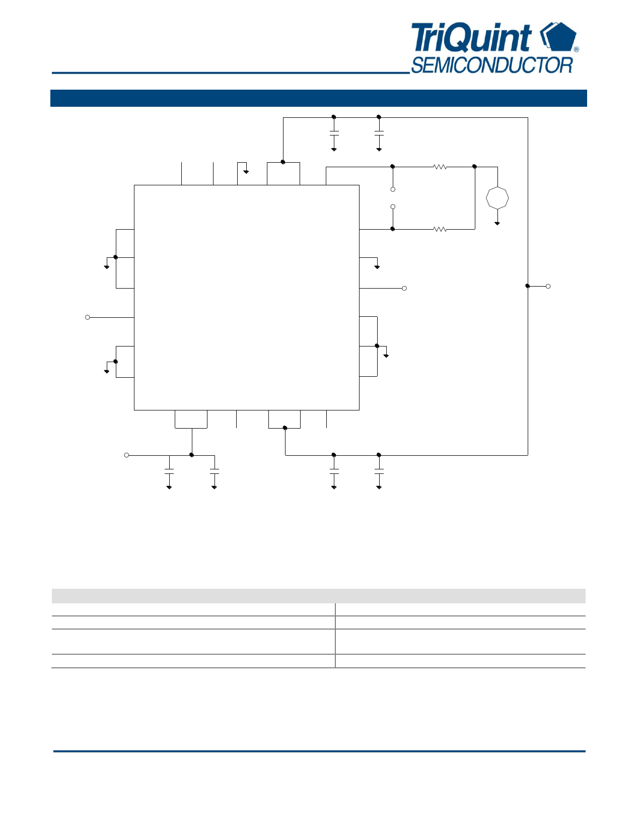
Application Circuit
C1
100 pF
24 23 22 21 20 19
1
2
3
J1
4
RF IN
5
6
2533
YYWW
XXXX
C4
1 uF
Vdet
Vdiff
18
Vref
17
R1
100K Ohms
R2
100K Ohms
16
J2
RF OUT
15
14
13
+_ 6 V
Vd = 6 V
Id = 1.3 A
7 8 9 10 11 12
Vg = -0.55 V
Typical
C2
C5
100 pF
1 uF
C3
C6
100 pF
1 uF
Vg can be biased from either side (pins 7 and 8 or pins 23 and 24), and the non-biased side can be left open.
Vd must be biased from both sides (pins 10, 11, 20, and 21).
Bias-up Procedure
Vg set to -1.5 V
Vd set to +6 V
Adjust Vg more positive until quiescent Id is 1.3A.
This will be ~ Vg = -0.55 V
Apply RF signal to RF Input
Bias-down Procedure
Turn off RF supply
Reduce Vg to -1.5V. Ensure Id ~ 0 mA
Turn Vd to 0 V
Turn Vg to 0 V
The TGA2533-SM will be marked with the “2533” designator and a lot code marked below the part designator. The “YY”
represents the last two digits of the year the part was manufactured, the “WW” is the work week, and the “XXXX” is an auto-
generated number.
Data Sheet: Rev D 11/05/13
© 2013 TriQuint Semiconductor, Inc.
- 7 of 13 -
Disclaimer: Subject to change without notice
Connecting the Digital World to the Global Network®