AD9954(Rev0) データシートの表示(PDF) - Analog Devices
部品番号
コンポーネント説明
メーカー
AD9954 Datasheet PDF : 36 Pages
| |||
ABSOLUTE MAXIMUM RATINGS
Table 2.
Parameter
Maximum Junction Temperature
DVDD_I/O (Pin 43)
AVDD, DVDD
Digital Input Voltage (DVDD_I/O = 3.3 V)
Digital Input Voltage (DVDD_I/O = 1.8 V)
Digital Output Current
Storage Temperature
Operating Temperature
Lead Temperature (10 sec Soldering)
θJA
θJC
Rating
150°C
4V
2V
–0.7 V to +5.25 V
–0.7 V to +2.2 V
5 mA
–65°C to +150°C
–40°C to +105°C
300°C
38°C/W
15°C/W
Stresses above those listed under Absolute Maximum Ratings
may cause permanent damage to the device. This is a stress rat-
ing only and functional operation of the device at these or any
other conditions above those indicated in the operational sec-
tion of this specification is not implied. Exposure to absolute
maximum rating conditions for extended periods may affect
device reliability.
AD9954
Table 3. Explanation of Test Levels
I 100% Production Tested.
II 100% Production Tested at 25°C and sample Tested at
Specified Temperatures.
III Sample Tested Only.
IV Parameter is guaranteed by design and characterization
testing.
V Parameter is a typical value only.
VI Devices are 100% production tested at 25°C and
guaranteed by design and characterization testing for
industrial operating temperature range.
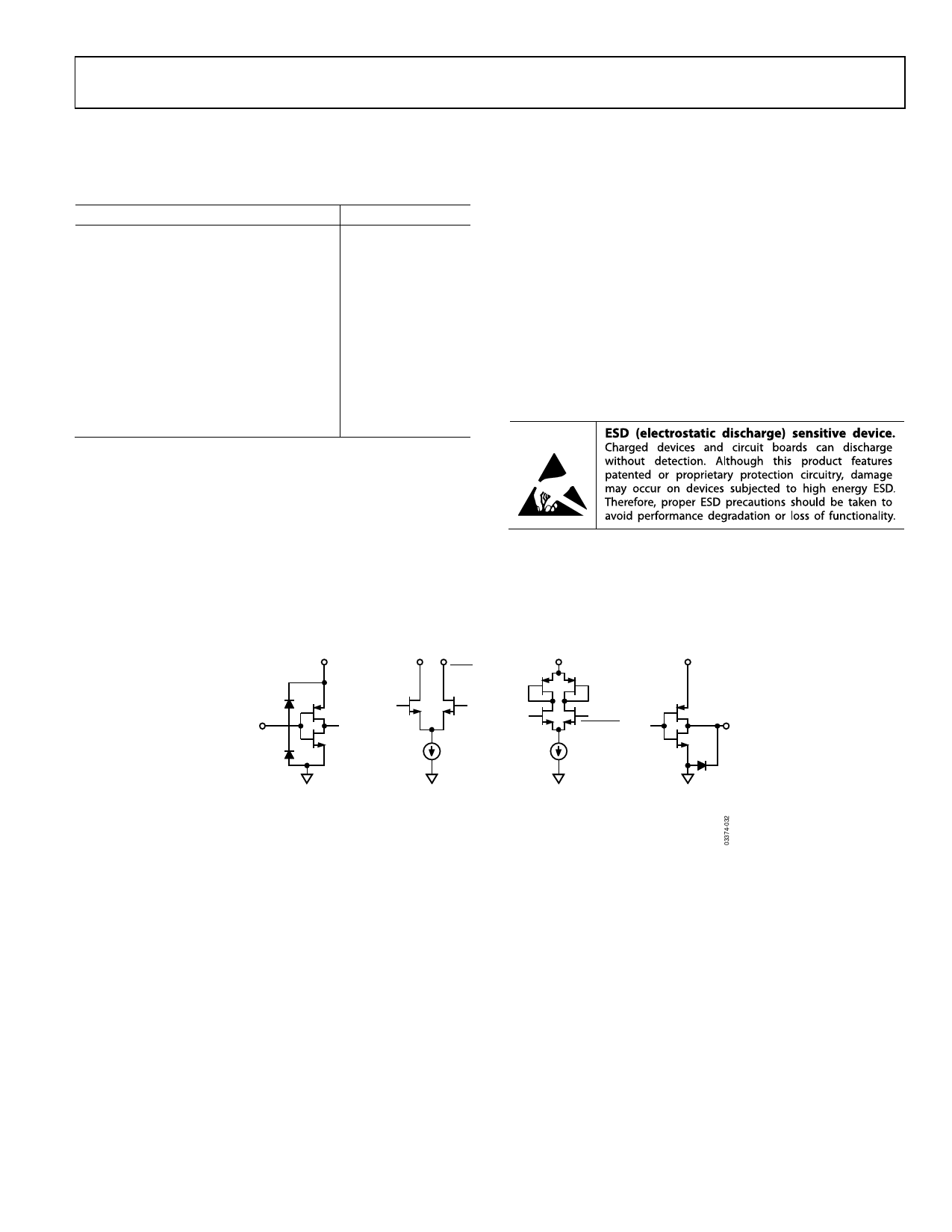
DIGITAL
INPUTS
DVDD_I/O
DAC OUTPUTS
IOUT
IOUT
INPUT
COMPARATOR
INPUTS
AVDD
COMP IN
COMP IN
COMPARATOR
OUTPUT
AVDD
AVOID OVERDRIVING
DIGITAL INPUTS.
FORWARD BIASING
ESD DIODES MAY
COUPLE DIGITAL NOISE
ONTO POWER PINS.
MUST TERMINATE
OUTPUTS TO AVDD FOR
CURRENT FLOW. DO
NOT EXCEED THE
OUTPUT VOLTAGE
COMPLIANCE RATING.
Figure 2. Equivalent Input and Output Circuits
Rev. 0 | Page 7 of 36
Share Link: 