ADSP-BF538BBCZ-4A гГЗгГЉгВњгВЈгГЉгГИгБЃи°®з§ЇпЉИPDFпЉЙ - Analog Devices
йГ®еУБзХ™еПЈ
гВ≥гГ≥гГЭгГЉгГНгГ≥гГИи™ђжШО
гГ°гГЉгВЂгГЉ
ADSP-BF538BBCZ-4A Datasheet PDF : 56 Pages
| |||
ADSP-BF538/ADSP-BF538F
Preliminary Technical Data
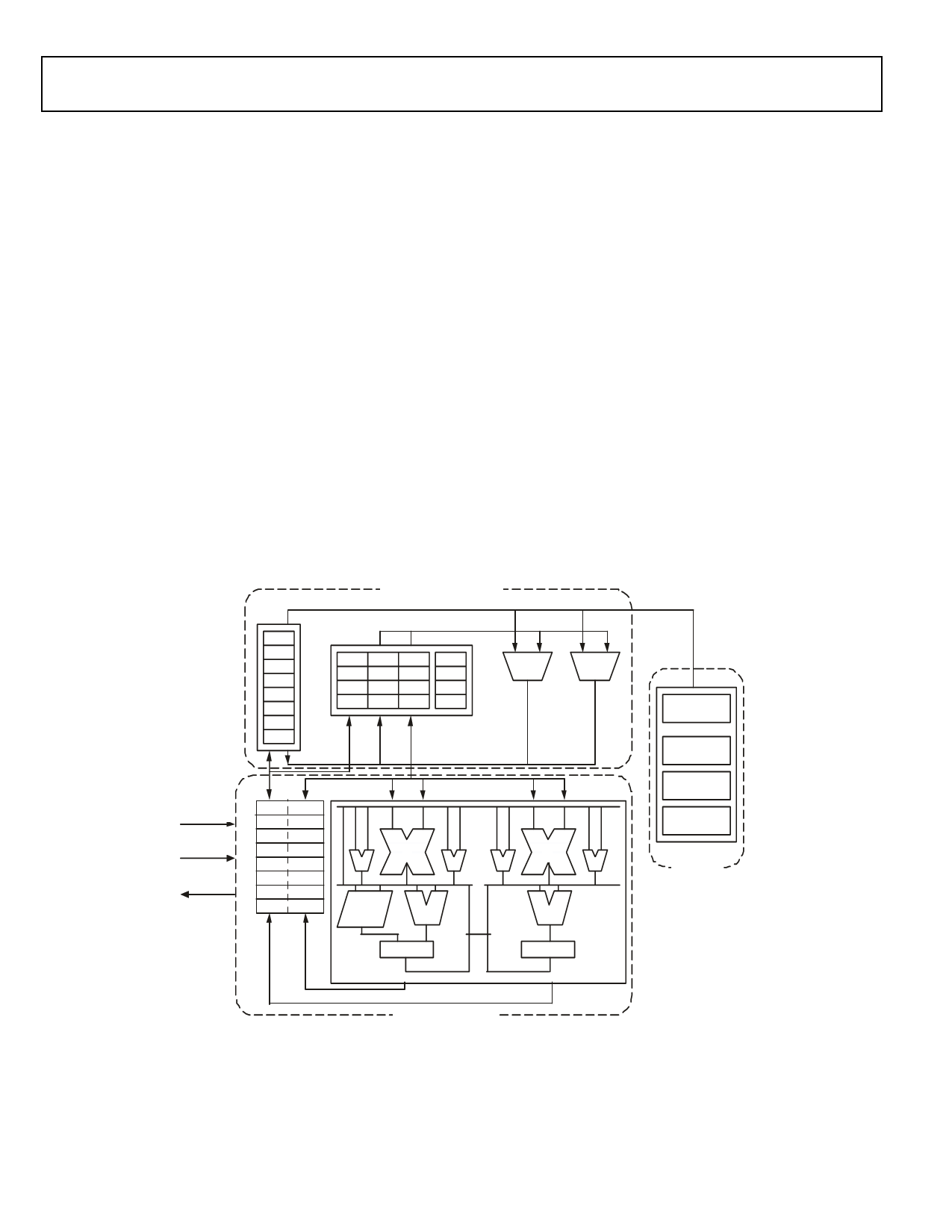
BLACKFIN PROCESSOR CORE
As shown in Figure 2 on Page 4, the Blackfin processor core
contains two 16-bit multipliers, two 40-bit accumulators, two
40-bit ALUs, four video ALUs, and a 40-bit shifter. The compu-
tation units process 8-bit, 16-bit, or 32-bit data from the register
file.
The compute register file contains eight 32-bit registers. When
performing compute operations on 16-bit operand data, the
register file operates as 16 independent 16-bit registers. All
operands for compute operations come from the multiported
register file and instruction constant fields.
Each MAC can perform a 16-bit by 16-bit multiply in each
cycle, accumulating the results into the 40-bit accumulators.
Signed and unsigned formats, rounding, and saturation are
supported.
The ALUs perform a traditional set of arithmetic and logical
operations on 16-bit or 32-bit data. In addition, many special
instructions are included to accelerate various signal processing
tasks. These include bit operations such as field extract and pop-
ulation count, modulo 232 multiply, divide primitives, saturation
and rounding, and sign/exponent detection. The set of video
instructions include byte alignment and packing operations, 16-
bit and 8-bit adds with clipping, 8-bit average operations, and 8-
bit subtract/absolute value/accumulate (SAA) operations. Also
provided are the compare/select and vector search instructions.
For certain instructions, two 16-bit ALU operations can be per-
formed simultaneously on register pairs (a 16-bit high half and
16-bit low half of a compute register). By also using the second
ALU, quad 16-bit operations are possible.
The 40-bit shifter can perform shifts and rotates and is used to
support normalization, field extract, and field deposit
instructions.
The program sequencer controls the flow of instruction execu-
tion, including instruction alignment and decoding. For
program flow control, the sequencer supports PC relative and
indirect conditional jumps (with static branch prediction), and
subroutine calls. Hardware is provided to support zero over-
head looping. The architecture is fully interlocked, meaning that
the programmer need not manage the pipeline when executing
instructions with data dependencies.
The address arithmetic unit provides two addresses for simulta-
neous dual fetches from memory. It contains a multiported
register file consisting of four sets of 32-bit index, modify,
length, and base registers (for circular buffering), and eight
additional 32-bit pointer registers (for C style indexed stack
manipulation).
ADDRESS ARITHMETIC UNIT
SP
FP
P5
I3 L3 B3
M3
DAG0
DAG1
I2 L2 B2
M2
P4
I1 L1 B1
M1
P3
I0 L0 B0
M0
P2
P1
P0
R7 R7.H R7.L
LD0 32 BITS R6 R6.H R6.L
R5 R5.H R5.L
LD1 32 BITS R4 R4.H R4.L
R3 R3.H R3.L
SD 32 BITS R2 R2.H R2.L
R1 R1.H R1.L
R0 R0.H R0.L
16
8
8
BARREL
SHIFTER
40
A0
16
8
8
40
A1
SEQUENCER
ALIGN
DECODE
LOOP BUFFER
CONTROL
UNIT
DATA ARITHMETIC UNIT
Figure 2. Blackfin Processor Core
Rev. PrD | Page 4 of 56 | May 2006
Share Link: 