CXD2450R データシートの表示(PDF) - Sony Semiconductor
部品番号
コンポーネント説明
メーカー
CXD2450R Datasheet PDF : 30 Pages
| |||
CXD2450R
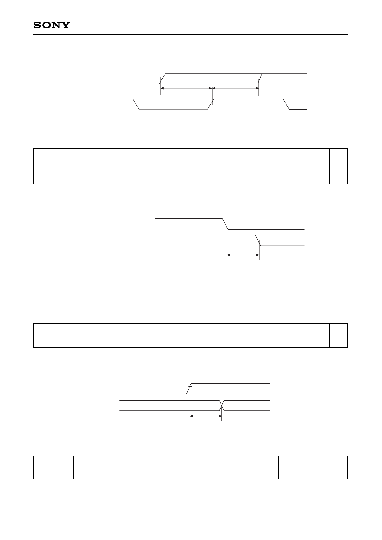
6) FRI and HRI loading characteristics
FRI, HRI
MCK
0.2VDDd
ts5
0.8VDDd
0.2VDDd
th5
MCK load capacitance = 10pF
(Within the recommended operating conditions)
Symbol
Definition
Miin. Typ. Min. Unit
ts5
FRI and HRI setup time, activated by the rising edge of MCK 10
ns
th5
FRI and HRI hold time, activated by the rising edge of MCK
0
ns
7) Output timing characteristics using DSGAT
DSGAT
H1, H2, RG, XSHP, XSHD, XRS,
PBLK, XCLPDM, XCLPOB, CLD
0.2VDDd
0.2VDDd
tpDSGAT
However, V2a, V2b and VSUB are fixed to the voltage level applied to the VH pin, and V1 and V3 are fixed to
the voltage level applied to the VM pin.
H1 and H2 load capacitance = 100pF, RG load capacitance = 20pF,
XSHP, XSHD, XRS, PBLK, XCLPDM, XCLPOB and CLD load capacitance = 10pF
(Within the recommended operating conditions)
Symbol
Definition
tpDSGAT Time until the above outputs go low after the fall of DSGAT
Miin. Typ. Min. Unit
100 ns
8) Output variation characteristics
MCK
0.8VDDd
WEN, ID
tpd2
WEN and ID load capacitance = 10pF
(Within the recommended operating conditions)
Symbol
tpd2
Definition
Time until the above outputs change after the rise of MCK
Miin. Typ. Min. Unit
20
40 ns
– 11 –
Share Link: 