MAX5104 データシートの表示(PDF) - Maxim Integrated
部品番号
コンポーネント説明
メーカー
MAX5104 Datasheet PDF : 12 Pages
| |||
Low-Power, Dual, Voltage-Output, 12-Bit DAC
with Serial Interface
_____________________Pin Description
PIN NAME
FUNCTION
1
AGND Analog Ground
2
OUTA DAC A Output Voltage
3
OSA DAC A Offset Adjustment
4
REFA Reference for DAC A
5
CL
Active-Low Clear Input. Resets all reg-
isters to zero. DAC outputs go to 0V.
6
CS
Chip-Select Input
7
DIN
Serial-Data Input
8
SCLK Serial-Clock Input
9
DGND Digital Ground
10
DOUT Serial-Data Output
11
UPO User-Programmable Output
12
PDL
Power-Down Lockout. The device can-
not be powered down when PDL is low.
13
REFB Reference for DAC B
14
OSB DAC B Offset Adjustment
15
OUTB DAC B Output Voltage
16
VDD
Positive Power Supply
_______________Detailed Description
The MAX5104 dual, 12-bit, voltage-output DAC is easily
configured with a 3-wire serial interface. The device
includes a 16-bit data-in/data-out shift register, and
each DAC has a double-buffered input composed of an
input register and a DAC register (see Functional
Diagram). In addition, trimmed internal resistors produce
an internal gain of +2V/V that maximizes output voltage
swing. The amplifier’s offset-adjust pin allows for a DC
shift in the DAC’s output.
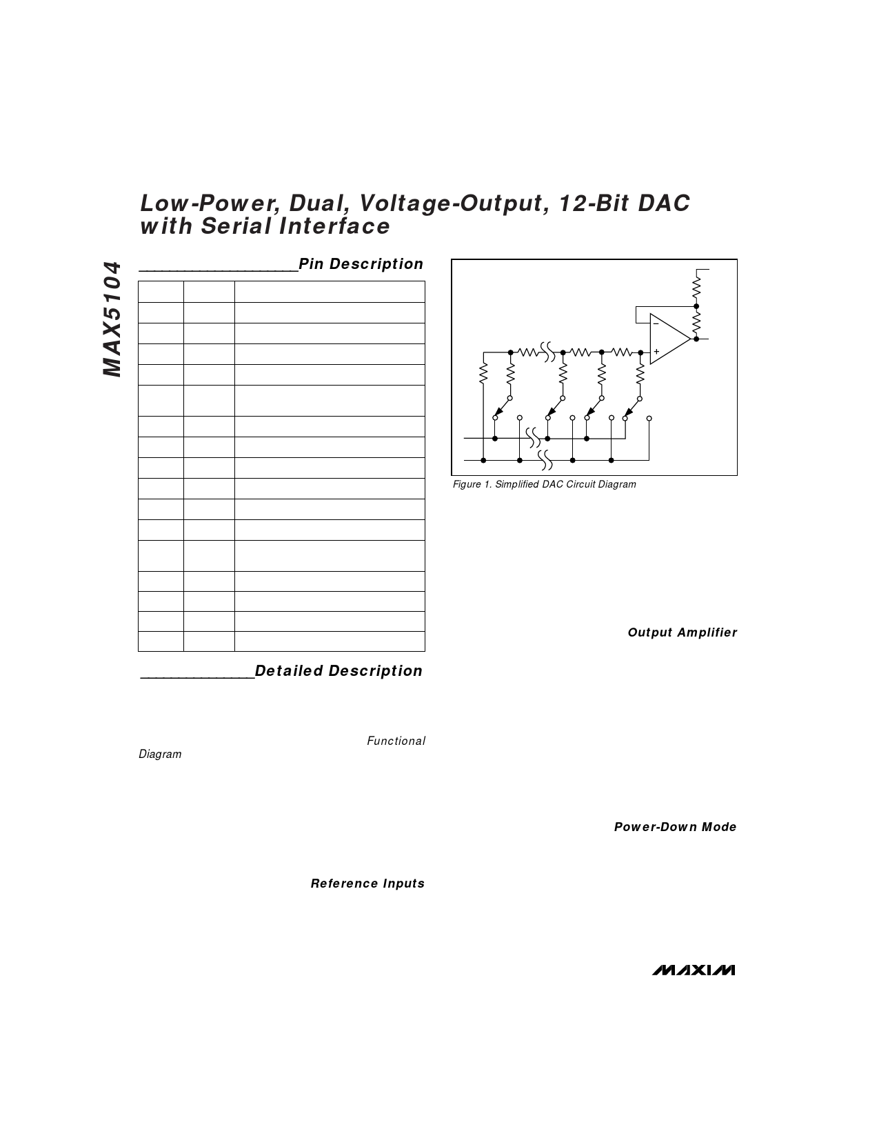
Both DACs use an inverted R-2R ladder network that
produces a weighted voltage proportional to the input
voltage value. Each DAC has its own reference input to
facilitate independent full-scale values. Figure 1 depicts
a simplified circuit diagram of one of the two DACs.
Reference Inputs
The reference inputs accept both AC and DC values
with a voltage range extending from 0 to (VDD - 1.4V).
Determine the output voltage using the following equa-
tion (OS_ = AGND):
R
2R 2R
D0
OS_
R
R
R
R
OUT_
2R
2R
2R
D10
D11
D12
REF_
AGND
Figure 1. Simplified DAC Circuit Diagram
VOUT = (VREF · NB / 4096) · 2
where NB is the numeric value of the DAC’s binary input
code (0 to 4095) and VREF is the reference voltage.
The reference input impedance ranges from 14kΩ (1554
hex) to several gigohms (with an input code of 0000
hex). The reference input capacitance is code depen-
dent and typically ranges from 15pF with an input code
of all zeros to 50pF with a full-scale input code.
Output Amplifier
The MAX5104’s output amplifiers have internal resistors
that provide for a gain of +2V/V when OS_ is connected
to AGND. These resistors are trimmed to minimize gain
error. The output amplifiers have a typical slew rate of
0.75V/µs and settle to 1/2LSB within 15µs, with a load
of 10kΩ in parallel with 100pF. Loads less than 2kΩ
degrade performance.
The OS_ pin can be used to produce an adjustable off-
set voltage at the output. For instance, to achieve a 1V
offset, apply -1V to the OS_ pin to produce an output
range from 1V to (1V + VREF · 2). Note that the DAC’s
output range is still limited by the maximum output voltage
specification.
Power-Down Mode
The MAX5104 features a software-programmable shut-
down mode that reduces the typical supply current to
2µA. The two DACs can be powered down indepen-
dently, or simultaneously using the appropriate pro-
gramming command. Enter power-down mode by
writing the appropriate input-control word (Table 1). In
power-down mode, the reference inputs and amplifier
outputs become high impedance, and the serial inter-
face remains active. Data in the input registers is saved,
6 _______________________________________________________________________________________
Share Link: 