MAX6880 データシートの表示(PDF) - Maxim Integrated
部品番号
コンポーネント説明
メーカー
MAX6880 Datasheet PDF : 19 Pages
| |||
Dual-/Triple-Voltage, Power-Supply
Sequencers/Supervisors
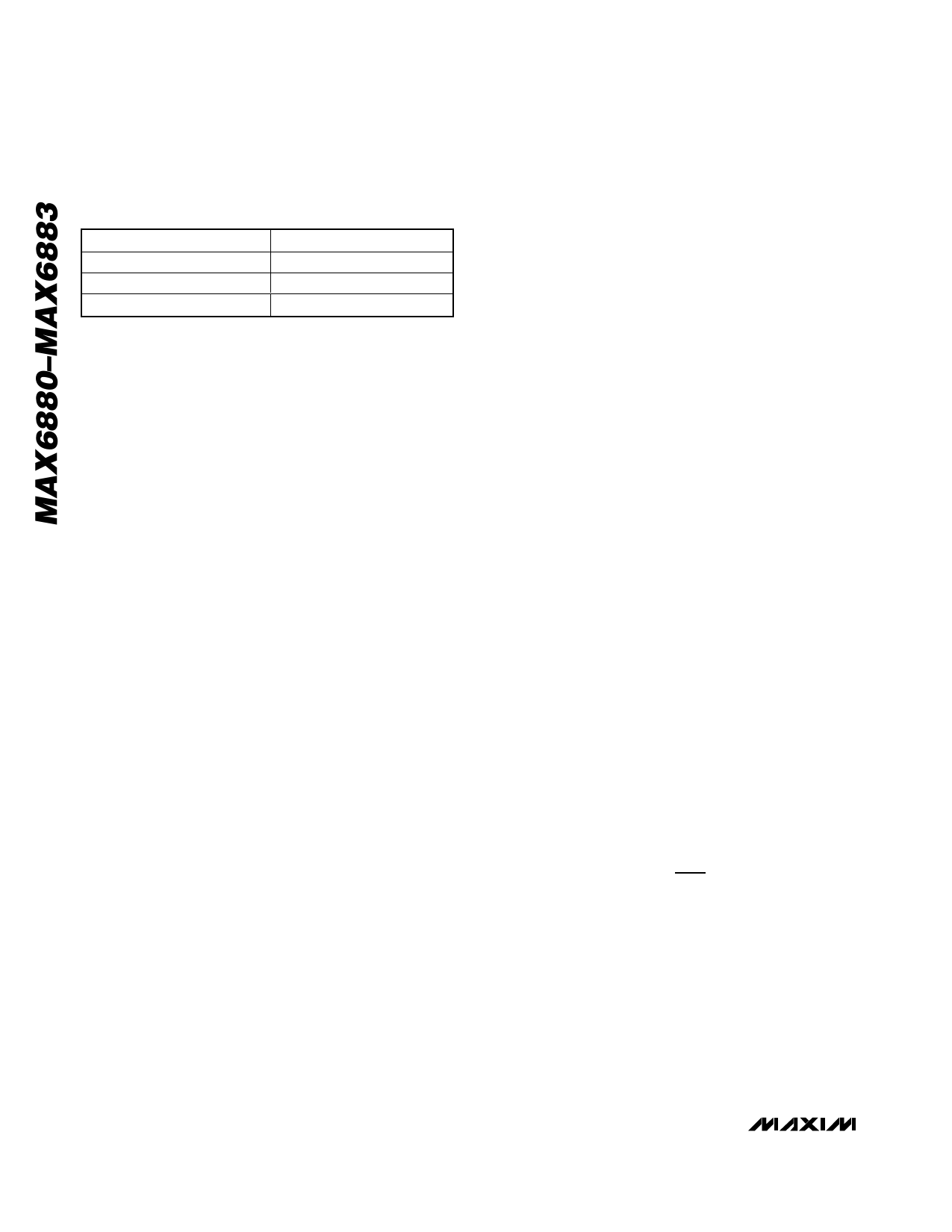
Table 1. CSLEW Timing Formulas
TIME PERIOD
Slew Rate
tRETRY
tFAULT
FORMULAS
(9.35 x 10⁻⁸) / CSLEW
3.506 x 10⁹ x CSLEW
2.191 x 10⁸ x CSLEW
Limiting Inrush Current
The capacitor (CSLEW) at SLEW to ground, controls the
OUT_ slew rate, thus controlling the inrush current
required to charge the load capacitor at OUT_. Using
the programmed slew rate, limit the inrush current by
using the following formula:
IINRUSH = COUT x SR
where IINRUSH is in amperes, COUT is in farads, and SR
is in V/s.
Delay Time Input (DELAY)
To adjust the desired delay period (tDELAY) before
sequencing is enabled, connect a capacitor (CDELAY)
between DELAY to ground (see Figures 2 to 5). The
selected delay time is also enforced when EN/UV rises
from low to high when all the input voltages are present.
Use the following formula to calculate the delay time:
tDELAY = 200µs + (500kΩ x CDELAY)
where tDELAY is in µs and CDELAY is in farads. Leave
DELAY unconnected for the default 200µs delay.
Timeout Period Input (TIMEOUT)
(MAX6880/MAX6882)
These devices feature a PG/RST timeout period.
Connect a capacitor (CTIMEOUT) from TIMEOUT to
ground to program the PG/RST timeout period. After all
OUT_ outputs exceed their IN_ referenced thresholds
(VTH_PG), PG/RST remains low for the selected timeout
period tTIMEOUT (see Figure 3).
tTIMEOUT = 200µs + (500kΩ x CTIMEOUT)
where tTIMEOUT is in µs and CTIMEOUT is in farads.
Leave TIMEOUT unconnected for the default 200µs
timeout delay.
Logic-Enable Input (EN/UV)
Drive logic EN/UV input above VEN_R to initiate voltage
sequencing during power-up operation. Drive logic
EN/UV below VEN_F to initiate tracking power-down
operation. Connect EN/UV to an external resistor-
divider network to set the external undervoltage lockout
threshold.
ABP Input (MAX6880/MAX6882)
ABP powers the analog circuitry. Bypass ABP to GND
with a 1µF ceramic capacitor installed as close to the
device as possible. ABP takes the highest voltage of
IN_. Do not use ABP to provide power to external cir-
cuitry. ABP maintains the device supply voltage during
rapid power-down conditions.
OUT1/OUT2/OUT3
The MAX6880/MAX6881 monitor three OUT_ and the
MAX6882/MAX6883 monitor two OUT_ outputs to con-
trol the sequencing performance. After the internal sup-
ply (ABP) exceeds the minimum voltage (2.7V)
requirements, EN/UV > VEN_R, and IN1/IN2/IN3 are all
greater than their adjusted SET_ thresholds, OUT1/
OUT2/OUT3 begin to sequence.
During fault conditions, an internal pulldown resistor
(100Ω) on OUT_ is enabled to help discharge load
capacitance (100Ω is connected for fast power-down
control).
Outputs
GATE_
The MAX6880–MAX6883 feature up to three GATE_ out-
puts to drive up to three external n-channel FET gates.
The following conditions must be met before GATE_
begins enhancing the external n-channel FET_:
1) All SET_ inputs (SET1/SET2/SET3) are above their
0.5V thresholds.
2) At least one IN_ input is above the minimum operat-
ing voltage (2.7V).
3) EN/UV > 1.25V.
At power-up mode, GATE_ voltages are enhanced by
control loops so all OUT_ voltages sequence at a
capacitor-adjusted slew rate. Each GATE_ is internally
pulled up to 5V above its relative IN_ voltage to fully
enhance the external n-channel FET when power-up is
complete.
Power-Good Output (PG/RST) (MAX6880/MAX6882)
The MAX6880/MAX6882 include a power-good (PG/RST)
output. PG/RST is an open-drain output and requires an
external pullup resistor.
All the OUT_ outputs must exceed their IN_ referenced
thresholds (IN_ x VTH_PG) for the selected reset timeout
period tTIMEOUT (see the TIMEOUT Period Input sec-
tion) before PG/RST asserts high. PG/RST stays low for
the selected reset timeout period (tTIMEOUT) after all
the OUT_ voltages exceed their IN_ referenced thresh-
olds. PG/RST goes low when VSET_ < VTH or VEN/UV <
VEN_R (see Figure 2).
14 ______________________________________________________________________________________
Share Link: 