EVAL-AD5750EBZ(RevF) データシートの表示(PDF) - Analog Devices
部品番号
コンポーネント説明
メーカー
EVAL-AD5750EBZ
(Rev.:RevF)
(Rev.:RevF)
Analog Devices

EVAL-AD5750EBZ Datasheet PDF : 36 Pages
| |||
Data Sheet
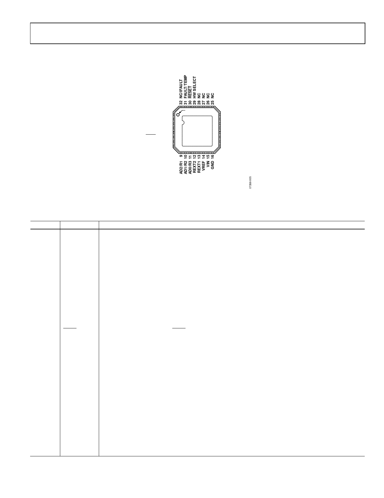
PIN CONFIGURATION AND FUNCTION DESCRIPTIONS
AD5750/AD5750-1/AD5750-2
SDO/VFAULT 1
CLRSEL 2
CLEAR 3
DVCC 4
GND 5
SYNC/RSET 6
SCLK/OUTEN 7
SDIN/R0 8
AD5750/
AD5750-1/
AD5750-2
TOP VIEW
(Not to Scale)
24 VSENSE+
23 VOUT
22 VSENSE–
21 AVSS
20 COMP1
19 COMP2
18 IOUT
17 AVDD
NOTES
1. NC = NO CONNECT.
2. THE EXPOSED PADDLE IS TIED TO AVSS.
Figure 4. Pin Configuration
Table 5. Pin Function Descriptions
Pin No. Mnemonic Description
1
SDO/VFAULT Serial Data Output (SDO). In software mode, this pin is used to clock data from the input shift register in
readback mode. Data is clocked out on the rising edge of SCLK and is valid on the falling edge of SCLK. This pin
is a CMOS output.
Short-Circuit Fault Alert (VFAULT). In hardware mode, this pin acts as a short-circuit fault alert pin and is
asserted low when a short-circuit error is detected. This pin is an open-drain output and must be connected to
a pull-up resistor.
2
CLRSEL
In hardware or software mode, this pin selects the clear value, either zero-scale or midscale code. In software
mode, this pin is implemented as a logic OR with the internal CLRSEL bit.
3
CLEAR
Active High Input. Asserting this pin sets the output current/voltage to zero-scale code or midscale code of the
range selected (user selectable). CLEAR is a logic OR with the internal clear bit.
In software mode, during power-up, the CLEAR pin level determines the power-on condition of the voltage
channel, which can be active 0 V or tristate. See the Asynchronous Clear (CLEAR) section for more details.
4
DVCC
Digital Power Supply.
5
GND
Ground Connection.
6
SYNC/RSET Positive Edge Sensitive Latch (SYNC). In software mode, a rising edge parallel loads the input shift register data
into the AD5750/AD5750-1/AD5750-2, also updating the output.
Resistor Select (RSET). In hardware mode, this pin selects whether the internal or the external current sense resistor is
used. If RSET = 0, the external sense resistor is chosen, and if RSET = 1, the internal sense resistor is chosen.
7
SCLK/OUTEN Serial Clock Input (SCLK). In software mode, data is clocked into the input shift register on the falling edge of
SCLK. This pin operates at clock speeds up to 50 MHz.
Output Enable (OUTEN). In hardware mode, this pin acts as an output enable pin.
8
SDIN/R0
Serial Data Input (SDIN). In software mode, data must be valid on the falling edge of SCLK.
Range Decode Bit (R0). In hardware mode, this pin, in conjunction with R1, R2, and R3, selects the output
current/voltage range setting on the part.
9
AD2/R1
Device Addressing Bit (AD2). In software mode, this pin, in conjunction with AD1 and AD0, allows up to eight
devices to be addressed on one bus.
Range Decode Bit (R1). In hardware mode, this pin, in conjunction with R0, R2, and R3, selects the output
current/voltage range setting on the part.
10
AD1/R2
Device Addressing Bit (AD1). In software mode, this pin, in conjunction with AD2 and AD0, allows up to eight
devices to be addressed on one bus.
Range Decode Bit (R2). In hardware mode, this pin, in conjunction with R0, R1, and R3, selects the output
current/voltage range setting on the part.
Rev. F | Page 11 of 36
Share Link: