GT15J331 データシートの表示(PDF) - Toshiba
部品番号
コンポーネント説明
メーカー
GT15J331 Datasheet PDF : 7 Pages
| |||
GT15J331
Electrical Characteristics (Ta = 25°C)
Characteristic
Symbol
Test Condition
Min
Gate leakage current
Collector cut-off current
Gate-emitter cut-off voltage
Collector-emitter saturation voltage
Input capacitance
Rise time
Switching time
Turn-on time
Fall time
Turn-off time
Peak forward voltage
Reverse recovery time
Thermal resistance (IGBT)
Thermal resistance (Diode)
IGES
VGE = ±20 V, VCE = 0
⎯
ICES
VCE = 600 V, VGE = 0
⎯
VGE (OFF) IC = 1.5 mA, VCE = 5 V
4.5
VCE (sat) IC = 15 A, VGE = 15 V
⎯
Cies
VCE = 20 V, VGE = 0, f = 1 MHz
⎯
tr
Inductive Load
ton
VCC = 300 V, IC = 15 A
tf
VGG = 15 V, RG = 43 Ω
toff
⎯
⎯
⎯
(Note1) ⎯
VF
IF = 15 A, VGE = 0
⎯
trr
IF = 15 A, di/dt = −100 A/μs
⎯
Rth (j-c)
⎯
⎯
Rth (j-c)
⎯
⎯
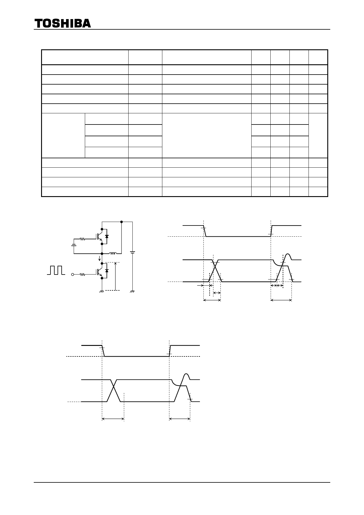
Note1: Switching time measurement circuit and input/output waveforms
Typ. Max Unit
⎯
⎯
⎯
1.75
2400
0.04
0.22
0.10
0.37
⎯
⎯
⎯
⎯
±500
1.0
7.5
2.3
⎯
⎯
⎯
0.23
⎯
2.0
200
1.79
3.45
nA
mA
V
V
pF
μs
V
ns
°C/W
°C/W
−VGE
IC
RG
L VCC
VCE
VGE
0
90%
IC
90%
0 VCE
10%
10%
td (off)
tf
toff
10%
90%
10%
td (on) tr
10%
ton
Note2: Switching loss measurement waveforms
VGE
0
90%
10%
IC
0 VCE
Eoff
5%
Eon
2
2006-10-31
Share Link: 