M29F100 データシートの表示(PDF) - STMicroelectronics
部品番号
コンポーネント説明
メーカー
M29F100 Datasheet PDF : 30 Pages
| |||
M29F100T, M29F100B
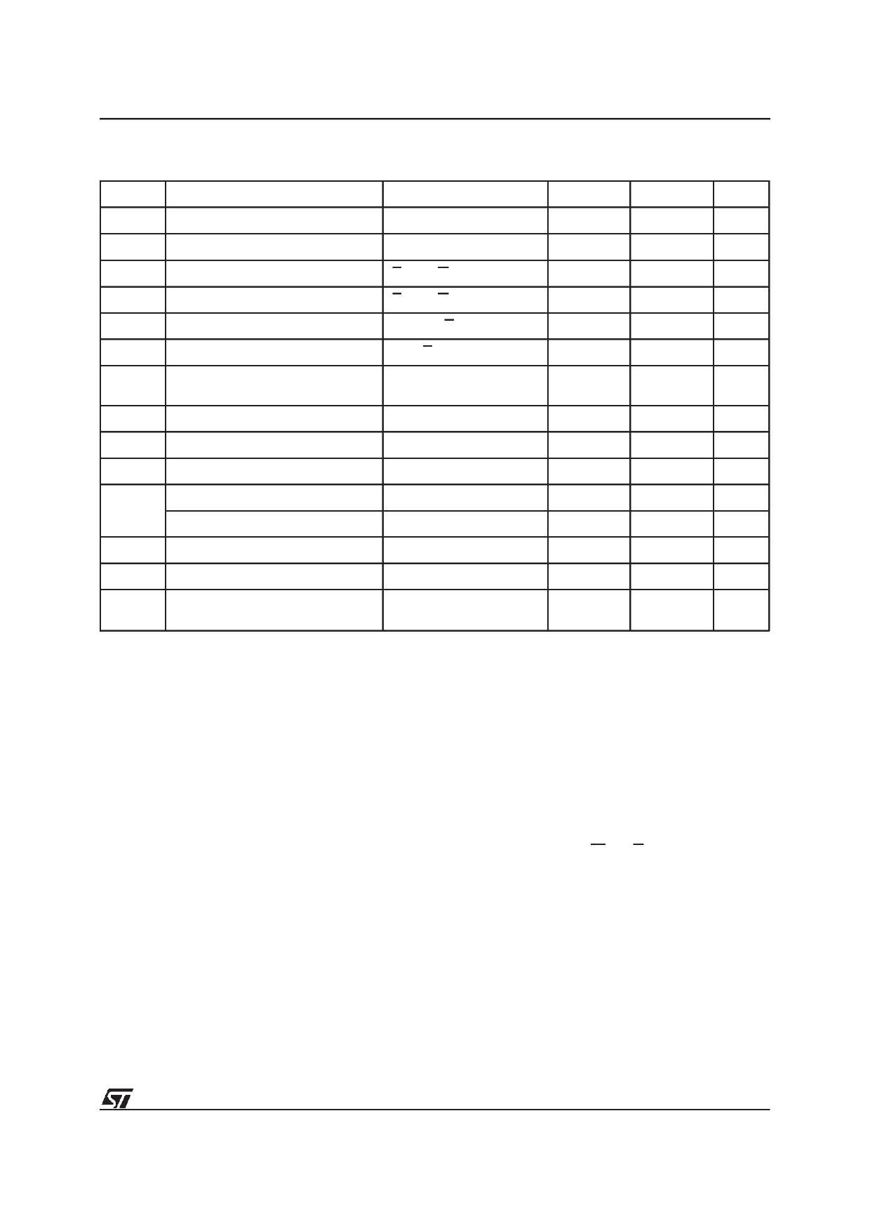
Table 13. DC Characteristics
(TA = 0 to 70°C, –40 to 85°C or –40 to 125°C; VCC = 5V ± 10%)
Symbol
Parameter
ILI
Input Leakage Current
ILO
Output Leakage Current
ICC1 Supply Current (Read) TTL Byte
ICC1 Supply Current (Read) TTL Word
ICC2 Supply Current (Standby) TTL
ICC3 Supply Current (Standby) CMOS
ICC4 (1) Supply Current (Program or Erase)
VIL
Input Low Voltage
VIH
Input High Voltage
VOL Output Low Voltage
Output High Voltage TTL
VOH
Output High Voltage CMOS
VID
A9 Voltage (Electronic Signature)
IID
A9 Current (Electronic Signature)
VLKO
Supply Voltage (Erase and
Program lock-out)
Note: 1. Sampled only, not 100% tested.
Test Condition
0V ≤ VIN ≤ VCC
0V ≤ VOUT ≤ VCC
E = VIL, G = VIH, f = 6MHz
E = VIL, G = VIH, f = 6MHz
E = VIH
E = VCC ± 0.2V
Byte program, Block or
Chip Erase in progress
IOL = 5.8mA
IOH = –2.5mA
IOH = –100µA
A9 = VID
Min
–0.5
2
2.4
VCC –0.4V
11.0
3.2
Max
±1
±1
20
20
1
100
20
0.8
VCC + 0.5
0.45
12.0
100
4.2
Unit
µA
µA
mA
mA
mA
µA
mA
V
V
V
V
V
V
µA
V
During the executionof the erase by the P/E.C., the
memory accepts only the Erase Suspend ES and
Read/Reset RD instructions. Data Polling bit DQ7
returns ’0’ while the erasure is in progress and ’1’
when it has completed. The Toggle bit DQ2 and
DQ6 toggle during the erase operation. They stop
when erase is completed. After completion the
Status Register bit DQ5 returns’1’ if there has been
an erase failure. In such a situation, the Toggle bit
DQ2 can be used to determine which block is not
correctly erased. In the case of erase failure, a
Read/Reset RD instruction is necessary in order to
reset the P/E.C.
ChipErase (CE) Instruction. This instructionuses
six write cycles. The Erase Set-up command 80h
is written to address AAAAh in the Byte-wide con-
figuration or the address 5555h in the Word-wide
configurationon the third cycle after the two Coded
cycles. The Chip Erase Confirm command 10h is
similarly written on the sixth cycle after anothertwo
Coded cycles. If the second command given is not
an erase confirm or if the Coded cycles are wrong,
the instruction aborts and the device is reset to
Read Array. It is not necessaryto programthe array
with 00h firstas theP/E.C. will automaticallydo this
before erasing it to FFh. Read operations after the
sixth rising edge of W or E output the Status
Register bits. During the execution of the erase by
the P/E.C., Data Polling bit DQ7 returns ’0’, then ’1’
on completion. The Toggle bits DQ2 and DQ6
toggle during erase operation and stop when erase
is completed. After completion the Status Register
bit DQ5 returns ’1’ if there has been an Erase
Failure.
13/30
Share Link: 