MACH120-18JI データシートの表示(PDF) - Lattice Semiconductor
部品番号
コンポーネント説明
メーカー
MACH120-18JI Datasheet PDF : 20 Pages
| |||
ABSOLUTE MAXIMUM RATINGS
Storage Temperature . . . . . . . . . . . . . -65°C to +150°C
Ambient Temperature
With Power Applied . . . . . . . . . . . . . .-55°C to +125°C
Device Junction Temperature . . . . . . . . . . . . . +150°C
Supply Voltage with
Respect to Ground . . . . . . . . . . . . . . -0.5 V to +7.0 V
DC Input Voltage . . . . . . . . . . . -0.5 V to VCC + 0.5 V
DC Output or I/O
Pin Voltage . . . . . . . . . . . . . . . . . -0.5 V to VCC + 0.5 V
Static Discharge Voltage . . . . . . . . . . . . . . . . . 2001 V
Latchup Current
(TA = 0°C to 70°C) . . . . . . . . . . . . . . . . . . . . 200 mA
Stresses above those listed under Absolute Maximum Ratings
may cause permanent device failure. Functionality at or above
these limits is not implied. Exposure to Absolute Maximum Rat-
ings for extended periods may affect device reliability. Pro-
gramming conditions may differ.
OPERATING RANGES
Commercial (C) Devices
Ambient Temperature (TA)
Operating in Free Air . . . . . . . . . . . . . . . 0°C to +70°C
Supply Voltage (VCC) . . . . . . . . . . . . . . . . . . . . . . . . .
with Respect to Ground . . . . . . . . . +4.75 V to +5.25 V
Operating ranges define those limits between which the func-
tionality of the device is guaranteed.
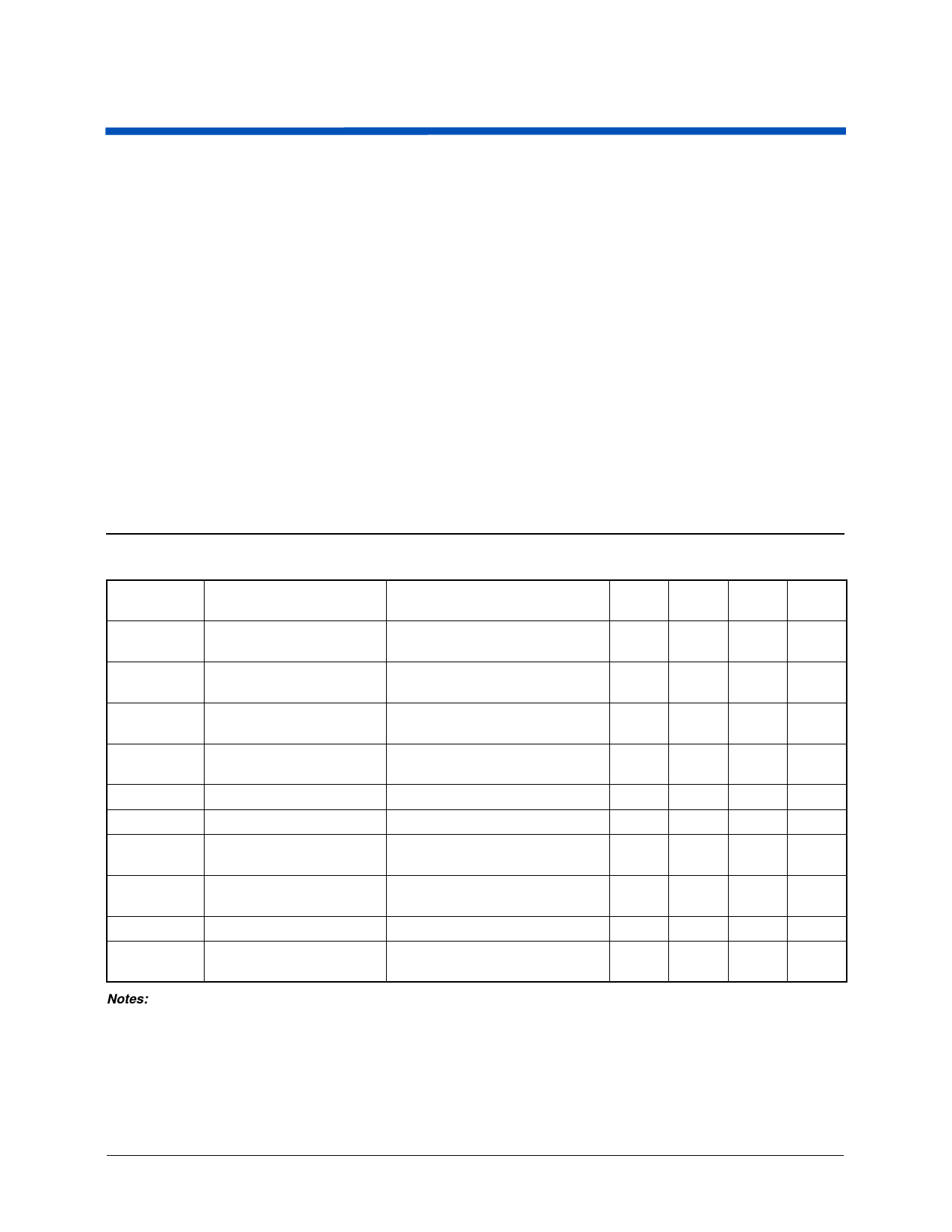
DC CHARACTERISTICS over COMMERCIAL operating ranges
Parameter
Symbol
VOH
VOL
VIH
VIL
IIH
IIL
IOZH
IOZL
ISC
ICC
Parameter Description
Output HIGH Voltage
Output LOW Voltage
Input HIGH Voltage
Input LOW Voltage
Input HIGH Current
Input LOW Current
Off-State Output Leakage
Current HIGH
Off-State Output Leakage
Current LOW
Output Short-Circuit Current
Supply Current (Typical)
Test Conditions
IOH = -3.2 mA, VCC = Min
VIN = VIH or VIL
IOL = 16 mA, VCC = Min
VIN = VIH or VIL
Guaranteed Input Logical HIGH
Voltage for all Inputs (Note 1)
Guaranteed Input Logical LOW
Voltage for all Inputs (Note 1)
VIN = 5.25 V, VCC = Max (Note 2)
VIN = 0 V, VCC = Max (Note 2)
VOUT = 5.25 V, VCC = Max
VIN = VIH or VIL (Note 2)
VOUT = 0 V, VCC = Max
VIN = VIH or VIL (Note 2)
VOUT = 0.5 V, VCC = Max (Note 3)
VCC = 5 V, TA=25°C, f = 25 MHz
(Note 4)
Min
Typ
Max Unit
2.4
V
0.5
V
2.0
V
0.8
V
10
µA
-10
µA
10
µA
-10
µA
-30
-130
mA
85
mA
Notes:
1. These are absolute values with respect to device ground and all overshoots due to system and/or tester noise are included.
2. I/O pin leakage is the worst case of IIL and IOZL (or IIH and IOZH).
3. Not more than one output should be shorted at a time. Duration of the short-circuit should not exceed one second.
VOUT = 0.5 V has been chosen to avoid test problems caused by tester ground degradation.
4. Measured with a 12-bit up/down counter pattern. This pattern is programmed in each PAL block and capable of being loaded,
enabled, and reset.
10
MACH120-12/15 (Com’l)
Share Link: 