SP791 データシートの表示(PDF) - Signal Processing Technologies
部品番号
コンポーネント説明
メーカー
SP791 Datasheet PDF : 19 Pages
| |||
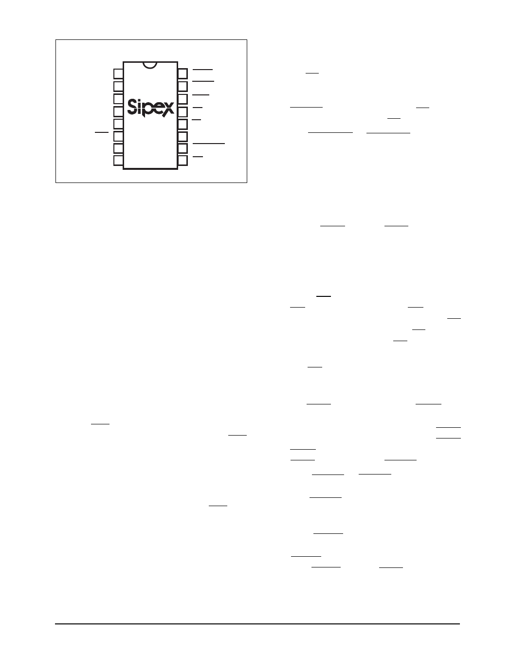
PINOUT
TOP VIEW
VBATT 1
VOUT 2
Vcc 3
GND 4
BATT ON 5
PFO 6
PFI 7
SWT 8
Corporation
DIP/SO
16 WDPO
15 RESET
14 WDO
13 CE IN
12 CE OUT
11 WDI
10 LOWLINE
9 MR
PIN ASSIGNMENTS
Pin 1 — V — Backup-Battery Input. Connect
BATT
to external battery or capacitor and charging
circuit.
Pin 2 —V — Output Supply Voltage. V con-
OUT
OUT
nects to VCC when VCC is greater than VBATT
and VCC is above the reset threshold. When
VCC falls below VBATT and VCC is below the
reset threshold, V connects to V . Con-
OUT
BATT
nect
a
0.1µF
capacitor
from
V
OUT
to
GND.
Pin 3 — V — Input Supply Voltage —
CC
+5V input
Pin 4 — GND — Ground reference for all signals
Pin 5 — BATT ON — Battery On Output. Goes
high when V switches to V . Goes low
OUT
BATT
when V switches to V . Connect the base
OUT
CC
of a PNP through a current-limiting resistor
to BATT ON for V current requirements
OUT
greater than 250mA.
Pin 6 — PFO — Power-Fail Output. This is the
output of the power-fail comparator. PFO
goes low when PFI is less than1.25V. This is
an uncommitted comparator, and has no ef-
fect on any other internal circuitry.
Pin 7 — PFI — Power-Fail Input. This is the
noninverting input to the power-fail compara-
tor. When PFI is less than 1.25V, PFO goes
low. Connect PFI to GND or V when not
OUT
used.
Pin 8 — SWT — Set Watchdog-Timeout Input.
Connect this input to V to select the de-
OUT
fault 1.6 sec watchdog timeout period. Con-
nect a capacitor between this input and GND
to select another watchdog-timeout period.
Watchdog-timeout period = 2.1 x (capacitor
value in nF) ms.
Pin 9 — MR — Manual-Reset Input. This input
can be tied to an external momentary
pushbutton switch, or to a logic gate output.
RESET remains low as long as MR is held
low and for 200ms after MR returns high.
Pin 10 — LOWLINE — LOWLINE Output goes
low when VCC falls to 150mV above the re-
set threshold. The output can be used to gen-
erate an NMI (nonmaskable interrupt) if the
unregulated supply is inaccessible.
Pin 11 — WDI — Watchdog Input. WDI is a three-
level input. If WDI remains either high or
low for longer than the watchdog timeout
period, WDO goes low. WDO remains low
until the next transition at WDI. Leaving
WDI unconnected disables the watchdog
function. WDI connects to an internal volt-
age divider between VOUT and GND, which
sets it to mid-supply when left unconnected.
Pin 12 — CE OUT — Chip-Enable Output.
CE OUT goes low only when CE IN is low
and VCC is above the reset threshold. If CE
IN is low when reset is asserted, CE OUT will
stay low for 15us or until CE IN goes high,
whichever occurs first.
Pin 13 — CE IN — Chip-Enable Input. The Input
to chip-enable gating circuit. Connect to
GND or VOUT if not used.
Pin 14 — WDO — Watchdog Output. WDO goes
low if WDI remains either high or low longer
than the watchdog timeout period. WDO
returns high on the next transition at WDI.
WDO remains high if WDI is unconnected.
WDO is also high when RESET is asserted.
Pin 15 — RESET — RESET Output goes low
whenever VCC falls below the reset thresh-
old. RESET will remain low for 200ms
after V crosses the reset threshold on
CC
power-up.
Pin 16 — WDPO — Watchdog-Pulse Output.
Upon the absence of a transition at WDI,
WDPO will pulse low for a minimum of
1ms. WDPO precedes WDO by 70ns.
SP791DS/08
SP791 Low Power Microprocessor Supervisory with Battery Switch-Over
5
© Copyright 2000 Sipex Corporation
Share Link: 