ML53612 データシートの表示(PDF) - Oki Electric Industry
部品番号
コンポーネント説明
メーカー
ML53612
Oki Electric Industry

ML53612 Datasheet PDF : 68 Pages
| |||
––––––––––––––––––––––––––––––––––––––––––––––––––––––––––––––––––––––––––––––––––– s ML53612 s
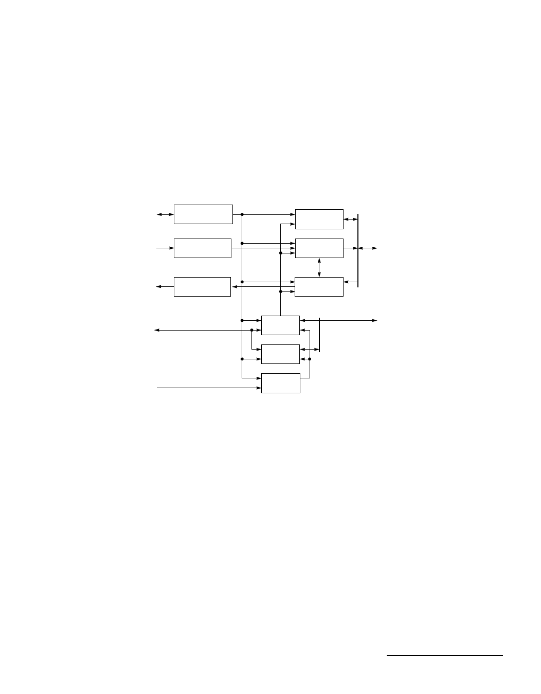
4.0 FUNCTIONAL DESCRIPTION
The ML53612 has the following interfaces:
• Microprocessor Interface
• Local Serial Data In
• Local Serial Data Out
• Local Timing
• Analog PLL Reference Clock
• CT Bus Timing
• CT Bus Serial Data
Microprocessor
Interface
Local Serial
Data In
Local Serial
Data Out
Local Timing
APLL
Reference Clock
Configuration &
Routing Register
Internal Control
64-Channel
Transmit Conversion
64-Channel
Receive Conversion
8 Channel
Stream Switch
64 x 4096
Transmit Switch
Local
Connect
4160 x 64
Receive Switch
Internal Timing
Slave Digital
PLL
Master
Digital PLL
Analog
PLL
131.072 MHz
Figure 2. Block Diagram
CT Bus Serial Data
CT Bus Timing
4.1 Local Bus
The local bus consists of up to two serial input ports and two serial output ports, totalling 128 possible
local bus connections to the CT Bus. The input and output ports can be configured independently as two
2 Mbps streams, one 4 Mbps stream, or one-half of an 8 Mbps stream. The chip includes two indepen-
dent, configurable local clock and frame synchronization signals. The local clocks have configurable
polarity and frequency that can be set to 2 MHz, 4 MHz, 8 MHz, or 16 MHz regardless of local stream
data rate. The local frame syncs also have a configurable polarity and can be set to use one of three fram-
ing formats (early, straddle, or late).
To transfer data to and from the local bus, the ML53612 allows the user to select a minimum delay or con-
stant delay buffer mode on a per channel basis. In the minimum delay mode, the input-output buffer
transfer occurs on the next 2 Mbps time-slot boundary, reducing any potential channel delay for classic
voice processing applications. In the constant delay mode, the buffer transfer occurs at the frame bound-
ary for bundling and proper switching of wide-band data, for data sent on the ISDN H channel.
Oki Semiconductor
7
Share Link: