X1228 データシートの表示(PDF) - Intersil
部品番号
コンポーネント説明
メーカー
X1228 Datasheet PDF : 29 Pages
| |||

X1228
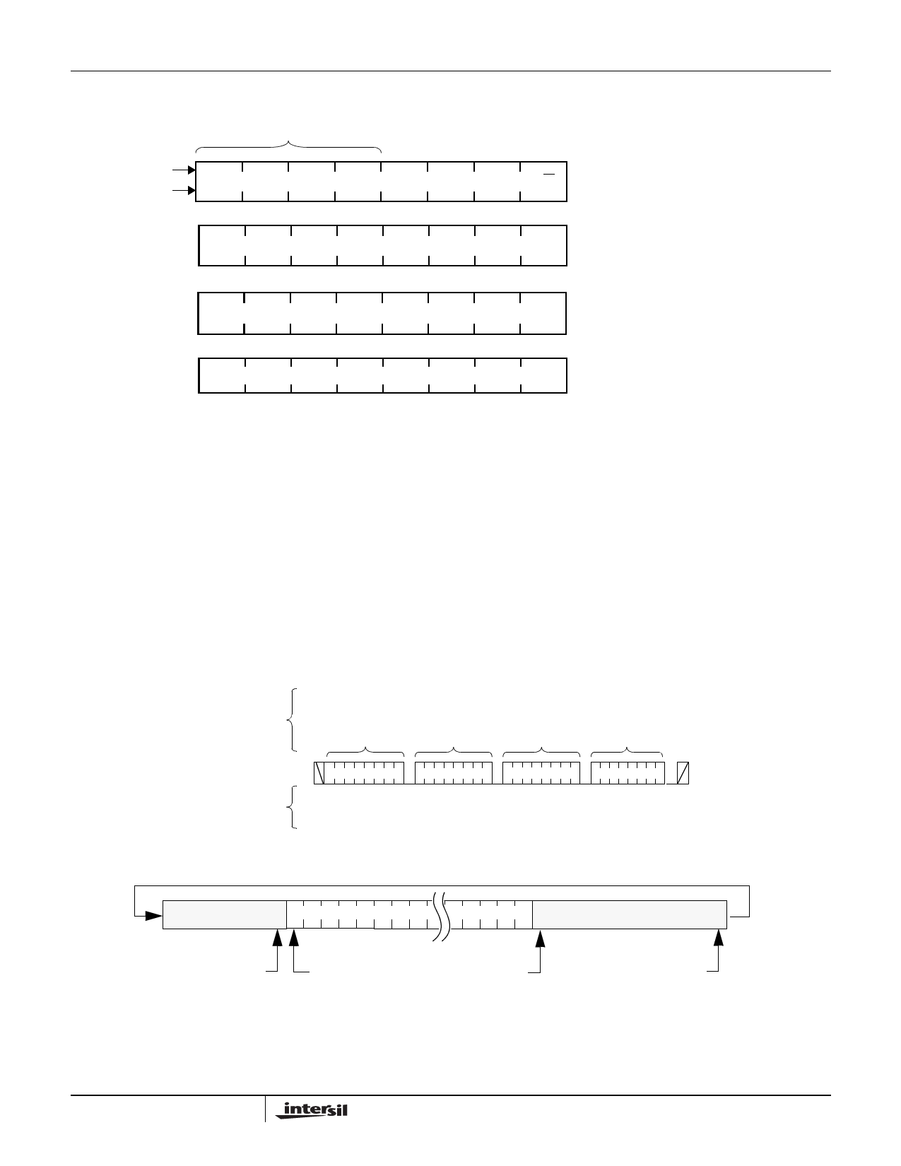
Figure 10. Slave Address, Word Address, and Data Bytes (64 Byte pages)
Device Identifier
Array
CCR
1
0
1
0
1
1
0
1
1
1
Slave Address Byte
1
R/W Byte 0
Word Address 1
0
0
0
0
0
0
0
A8
Byte 1
A7
A6
A5
A4
A3
A2
A1
A0
Word Address 0
Byte 2
Data Byte
D7
D6
D5
D4
D3
D2
D1
D0
Byte 3
Write Operations
Byte Write
For a write operation, the device requires the Slave
Address Byte and the Word Address Bytes. This gives
the master access to any one of the words in the array
or CCR. (Note: Prior to writing to the CCR, the master
must write a 02h, then 06h to the status register in two
preceding operations to enable the write operation.
See “Writing to the Clock/Control Registers.” Upon
receipt of each address byte, the X1228 responds with
an acknowledge. After receiving both address bytes
the X1228 awaits the eight bits of data. After receiving
the 8 data bits, the X1228 again responds with an
acknowledge. The master then terminates the transfer
by generating a stop condition. The X1228 then
begins an internal write cycle of the data to the nonvol-
atile memory. During the internal write cycle, the
device inputs are disabled, so the device will not
respond to any requests from the master. The SDA out-
put is at high impedance. See Figure 11.
Figure 11. Byte Write Sequence
Signals from
the Master
S
t
a
r
Slave
t Address
Word
Address 1
Word
Address 0
S
t
o
Data
p
SDA Bus
1
1 110 0000000
Signals From
The Slave
A
A
A
A
C
C
C
C
K
K
K
K
Figure 12. Writing 30 bytes to a 64-byte memory page starting at address 40.
7 Bytes
Address
=6
Address Pointer
Ends Here
Addr = 7
Address
40
23 Bytes
Address
63
20
FN8100.4
May 18, 2006