FM4005 データシートの表示(PDF) - Ramtron International Corporation
部品番号
コンポーネント説明
メーカー
FM4005 Datasheet PDF : 23 Pages
| |||
FM4005
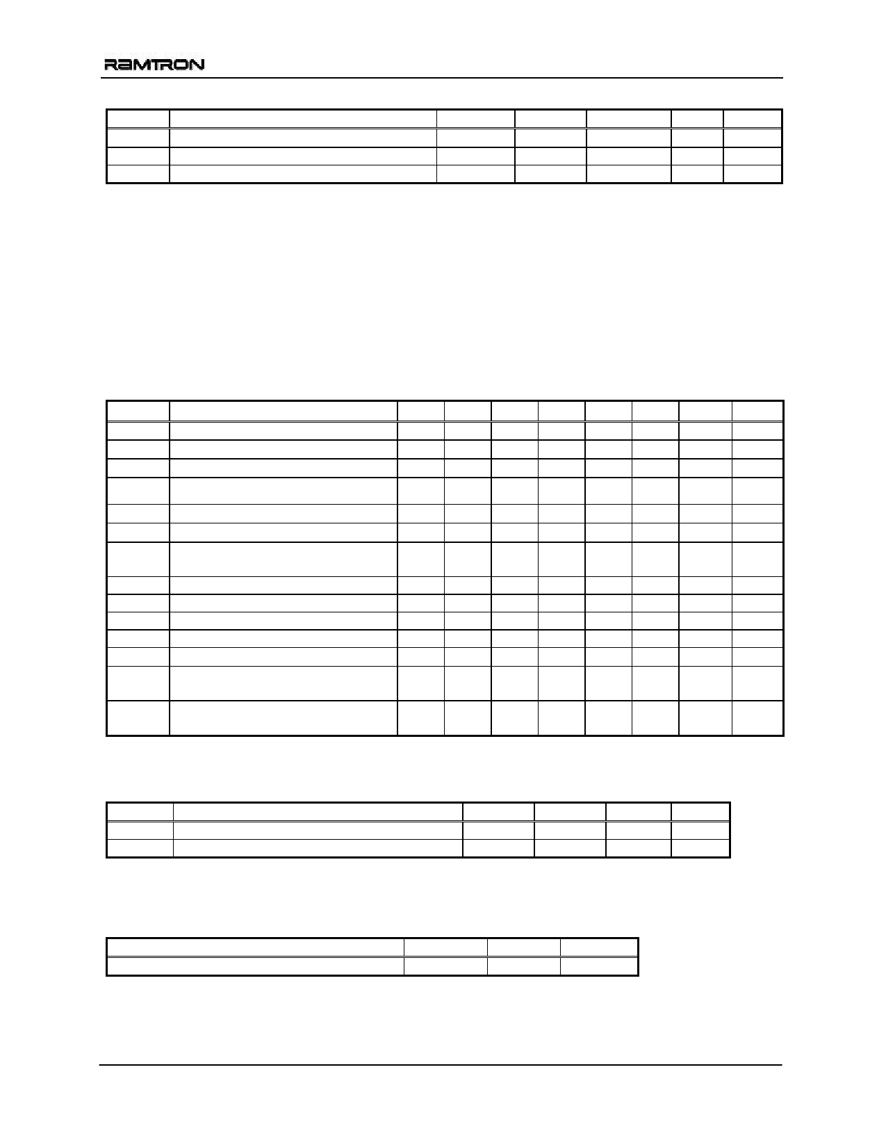
DC Operating Conditions, continued (TA = -40° C to + 85° C, VDD = 2.7V to 5.5V unless otherwise specified)
Symbol Parameter
Min
Typ
Max
Units Notes
RRST
Pull-up resistance for /RST Inactive
50
400
KΩ
VPFI
Power Fail Input Reference Voltage
1.175
1.20
VHYS Power Fail Input (PFI) Hysteresis (Rising)
-
1.225
V
100
mV
Notes
1. SCL toggling between VDD-0.3V and VSS, other inputs VSS or VDD-0.3V.
2. All inputs at VSS or VDD, static. Stop command issued.
3. VIN or VOUT = VSS to VDD. Does not apply to PFI or /RST pins.
4. VBAK = 3.0V, VDD < 2.4V, oscillator running, CNT1-2 at VBAK.
5. /RST is asserted active when VDD < VTP.
6. The minimum VDD to guarantee the level of /RST remains a valid VOL level.
7. Full complete operation. Supervisory circuits, RTC, etc operate to lower voltages as specified.
8. Includes /RST input detection of external reset condition to trigger driving of /RST signal by FM4005.
9. The VBAK trickle charger automatically regulates the maximum voltage on this pin for capacitor backup applications.
10. VBAK will source current when trickle charger is enabled (VBC bit=1), VDD > VBAK, and VBAK < VBAK max.
AC Parameters (TA = -40° C to + 85° C, VDD = 2.7V to 5.5V, CL = 100 pF unless otherwise specified)
Symbol
Parameter
Min Max Min Max Min Max
fSCL
tLOW
tHIGH
tAA
SCL Clock Frequency
Clock Low Period
Clock High Period
SCL Low to SDA Data Out Valid
0 100 0 400 0 1000
4.7
1.3
0.6
4.0
0.6
0.4
3
0.9
0.55
tBUF
Bus Free Before New Transmission 4.7
tHD:STA Start Condition Hold Time
4.0
1.3
0.5
0.6
0.25
tSU:STA Start Condition Setup for Repeated 4.7
Start
0.6
0.25
tHD:DAT
tSU:DAT
tR
tF
tSU:STO
tDH
Data In Hold
Data In Setup
Input Rise Time
Input Fall Time
Stop Condition Setup
Data Output Hold
(from SCL @ VIL)
0
0
0
250
100
100
1000
300
300
300
300
100
4.0
0.6
0.25
0
0
0
tSP
Noise Suppression Time Constant
on SCL, SDA
50
50
50
Notes: All SCL specifications as well as start and stop conditions apply to both read and write operations.
1. This parameter is characterized but not tested.
Units
kHz
µs
µs
µs
µs
µs
µs
ns
ns
ns
ns
µs
ns
ns
Notes
1
1
Capacitance (TA = 25° C, f=1.0 MHz, VDD = 3.0V)
Symbol
Parameter
Typ
CIO
Input/Output Capacitance
-
CXTAL X1, X2 Crystal Pin Capacitance
12
Notes
1 This parameter is characterized but not tested.
2 The crystal attached to the X1/X2 pins must be rated as 6pF.
Max
Units Notes
8
pF
1
pF
1, 2
Data Retention (TA = -40° C to + 85° C, VDD = 2.7V to 5.5V)
Parameter
Min
Data Retention (S/N and other NV bits)
10
Units
Years
Notes
Rev. 2.3
Oct. 2006
Page 19 of 23
Share Link: 