MACH211SP-10YC データシートの表示(PDF) - Lattice Semiconductor
部品番号
コンポーネント説明
メーカー
MACH211SP-10YC Datasheet PDF : 48 Pages
| |||
The flip-flops in either macrocell type can be clocked by one of several clock pins (Table 10).
Registers are clocked on the rising edge of the clock input. Latches hold their data when the gate
input is HIGH. Clock pins are also available as inputs, although care must be taken when a signal
acts as both clock and input to the same device.
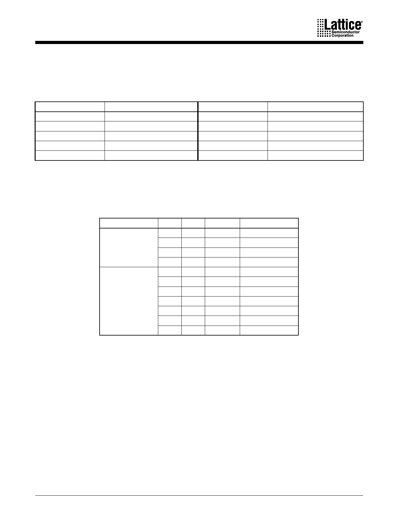
Table 10. Macrocell Clocks
Device
MACH111
MACH111SP
MACH131
MACH131SP
MACH211
Number of Clocks Available
4
2
4
4
4
Device
MACH211SP
MACH221
MACH221SP
MACH231
MACH231SP
Number of Clocks Available
2
4
4
4
4
All flip-flops have asynchronous reset and preset. This is controlled by the common product terms
that control all flip-flops within a PAL block. For a single PAL block, all flip-flops, whether in an
output or a buried macrocell, are initialized together. The initialization functionality of the flip-flops
is illustrated in Table 11.
Table 11. Asynchronous Reset/Preset Operation
Configuration
Register
Latch
AR
AP
0
0
0
1
1
0
1
1
0
0
0
1
0
1
1
0
1
0
1
1
1
1
CLK/LE
X
X
X
X
X
0
1
0
1
0
1
Q+
See Table 9
1
0
0
See Table 9
Illegal
1
Illegal
0
Illegal
0
I/O Cells
The I/O cells (Figure 7) provide a three-state output buffer. The three-state buffer can be left
permanently enabled for use only as an output, permanently disabled for use as an input, or it can
be controlled by one of two product terms for bi-directional signals and bus connections. The two
product terms provided are common to a bank of I/O cells.
MACH 1 & 2 Families
11
Share Link: 