M59DR032 データシートの表示(PDF) - STMicroelectronics
部品番号
コンポーネント説明
メーカー
M59DR032 Datasheet PDF : 40 Pages
| |||
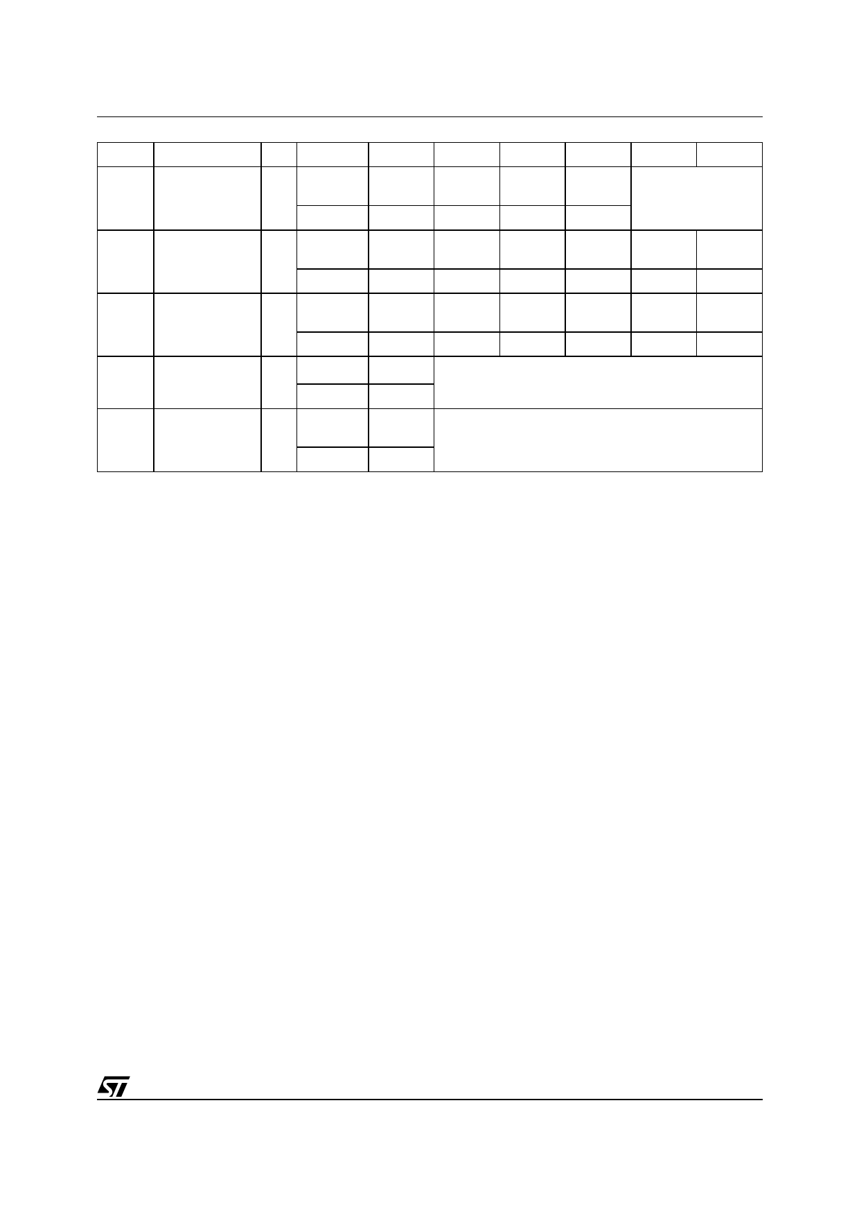
M59DR032A, M59DR032B
Mne.
Instr.
Cyc.
1st Cyc. 2nd Cyc. 3rd Cyc. 4th Cyc. 5th Cyc. 6th Cyc.
BL Block Lock
Addr.
4
Data
555h
AAh
2AAh
55h
555h
60h
Block
Address
2Fh
BE Block Erase
Addr.
6+
Data
555h
AAh
2AAh
55h
555h
80h
555h
AAh
2AAh
55h
Block
Address
30h
BKE Bank Erase
Addr.
6
Data
555h
AAh
2AAh
55h
555h
80h
555h
AAh
2AAh
55h
Bank
Address
10h
ES Erase Suspend
Addr. (3)
1
Data
X
Read until Toggle stops, then read all the data needed
B0h from any Blocks not being erased then Resume Erase.
ER Erase Resume
Addr.
1
Data
Bank
Address Read Data Polling or Toggle Bits until Erase completes or
Erase is suspended another time
30h
Note: 1. Commands not interpreted in this table will default to read array mode.
2. For Coded cycles address inputs A11-A20 are don’t care.
3. X = Don’t Care.
4. The first cycles of the RD or AS instructions are followed by read operations. Any number of read cycles can occur after the com-
mand cycles.
5. During Erase Suspend, Read and Data Program functions are allowed in blocks not being erased.
6. Program Address 1 and Program Address 2 must be consecutive addresses differing only for address bit A0.
7. High voltage on VPP (11.4V to 12.6V) is required for the proper execution of the Double Word Program instruction.
13/39
Share Link: 