M59DR032 データシートの表示(PDF) - STMicroelectronics
部品番号
コンポーネント説明
メーカー
M59DR032 Datasheet PDF : 40 Pages
| |||
M59DR032A, M59DR032B
COMMON FLASH INTERFACE (CFI)
The Common Flash Interface (CFI) specification is
a JEDEC approved, standardised data structure
that can be read from the Flash memory device.
CFI allows a system software to query the flash
device to determine various electrical and timing
parameters, density information and functions
supported by the device. CFI allows the system to
easily interface to the Flash memory, to learn
about its features and parameters, enabling the
software to configure itself when necessary.
Tables 18, 19, 20 and 21 show the address used
to retrieve each data.
The CFI data structure gives information on the
device, such as the sectorization, the command
set and some electrical specifications. Tables 18,
19, 20 and 21 show the addresses used to retrieve
each data. The CFI data structure contains also a
security area; in this section, a 64 bit unique secu-
rity number is written, starting at address 81h. This
area can be accessed only in read mode and there
are no ways of changing the code after it has been
written by ST. Write a read instruction to return to
Read mode. Refer to the CFI Query instruction to
understand how the M59DR032 enters the CFI
Query mode.
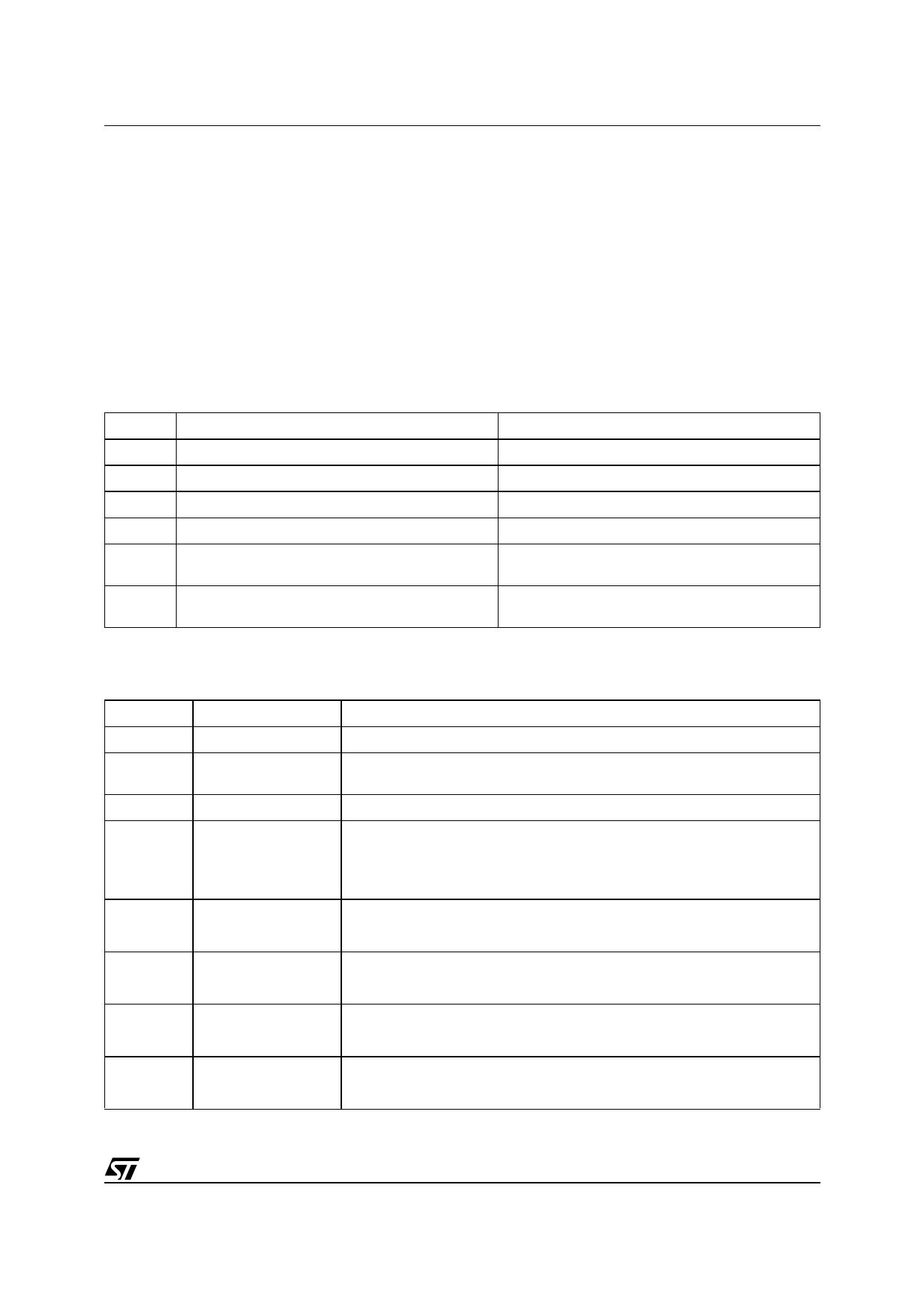
Table 18. Query Structure Overview
Offset
Sub-section Name
Description
00h Reserved
Reserved for algorithm-specific information
10h CFI Query Identification String
Command set ID and algorithm data offset
1Bh System Interface Information
Device timing & voltage information
27h Device Geometry Definition
Flash device layout
P
Primary Algorithm-specific Extended Query table
Additional information specific to the Primary
Algorithm (optional)
A
Alternate Algorithm-specific Extended Query table
Additional information specific to the Alternate
Algorithm (optional)
Note: The Flash memory display the CFI data structure when CFI Query command is issued. In this table are listed the main sub-sections
detailled in Tables 19, 20 and 21. Query data are always presented on the lowest order data outputs.
Table 19. CFI Query Identification String
Offset
Data
Description
00h
0020h
Manufacturer Code
01h
00A1h - bottom
00A0h - top
Device Code
02h-0Fh
reserved
Reserved
10h
0051h
Query Unique ASCII String "QRY"
11h
0052h
Query Unique ASCII String "QRY"
12h
0059h
Query Unique ASCII String "QRY"
13h
0002h
Primary Algorithm Command Set and Control Interface ID code 16 bit ID code
14h
0000h
defining a specific algorithm
15h
offset = P = 0040h
Address for Primary Algorithm extended Query table
16h
0000h
17h
0000h
Alternate Vendor Command Set and Control Interface ID Code second vendor
18h
0000h
- specified algorithm supported (note: 0000h means none exists)
19h
value = A = 0000h Address for Alternate Algorithm extended Query table
1Ah
0000h
note: 0000h means none exists
Note: Query data are always presented on the lowest - order data outputs (DQ7-DQ0) only. DQ8-DQ15 are ‘0’.
17/39
Share Link: 