M59DR032 データシートの表示(PDF) - STMicroelectronics
部品番号
コンポーネント説明
メーカー
M59DR032 Datasheet PDF : 40 Pages
| |||
M59DR032A, M59DR032B
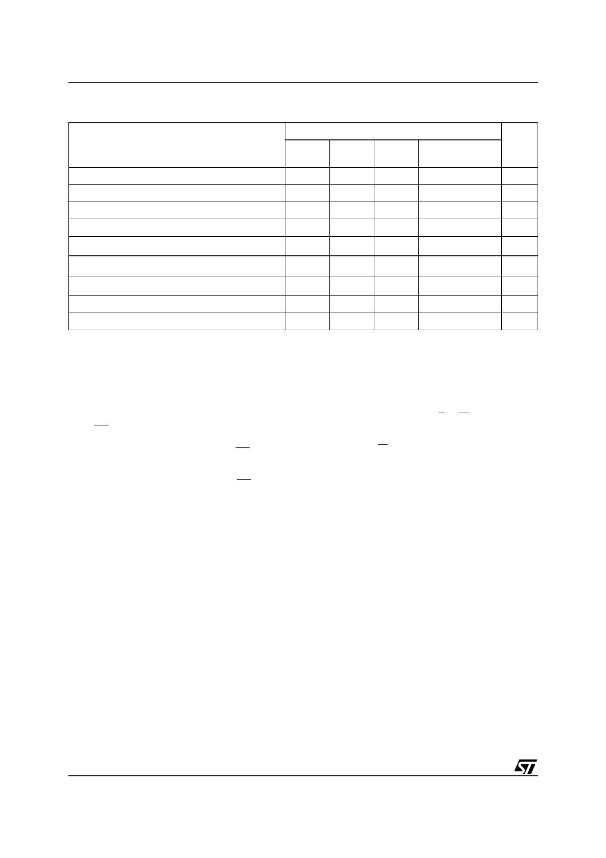
Table 17. Program, Erase Times and Program, Erase Endurance Cycles
(TA = 0 to 70°C; VDD = VDDQ = 1.65V to 2.2V, VPP = VDD unless otherwise specified)
M59DR032
Parameter
Min
Max (1)
Typ
Typical after
Unit
100k W/E Cycles
Parameter Block (4 KWord) Erase (Preprogrammed)
2.5
0.15
0.4
s
Main Block (32 KWord) Erase (Preprogrammed)
10
1
3
s
Bank Erase (Preprogrammed, Bank A)
2
6
s
Bank Erase (Preprogrammed, Bank B)
10
30
s
Chip Program (2)
20
25
s
Chip Program (DPG, VPP = 12V) (2)
10
s
Word Program (3)
200
10
10
µs
Double Word Program
200
10
10
µs
Program/Erase Cycles (per Block)
100,000
cycles
Note: 1. Max values refer to the maximum time allowed by the internal algorithm before error bit is set. Worst case conditions program or
erase should perform significantly better.
2. Excludes the time needed to execute the sequence for program instruction.
3. Same timing value if VPP = 12V
POWER CONSUMPTION
Power Down
The memory provides Reset/Power Down control
input RP. The Power Down function can be acti-
vated only if the relevant Configuration Register bit
is set to ’1’. In this case, when the RP signal is
pulled at VSS the supply current drops to typically
ICC2 (see Table 24), the memory is deselected and
the outputs are in high impedance.If RP is pulled
to VSS during a Program or Erase operation, this
operation is aborted in tPLQ7V and the memory
content is no longer valid (see Reset/Power Down
input description).
Power Up
The memory Command Interface is reset on Pow-
er Up to Read Array. Either E or W must be tied to
VIH during Power Up to allow maximum security
and the possibility to write a command on the first
rising edge of W.
Supply Rails
Normal precautions must be taken for supply volt-
age decoupling; each device in a system should
have the VDD rails decoupled with a 0.1µF capac-
itor close to the VDD, VDDQ and VSS pins. The PCB
trace widths should be sufficient to carry the re-
quired VDD program and erase currents.
16/39
Share Link: 