CY7C1482V33-200BZXC データシートの表示(PDF) - Cypress Semiconductor
部品番号
コンポーネント説明
メーカー
CY7C1482V33-200BZXC Datasheet PDF : 31 Pages
| |||
CY7C1480V33
CY7C1482V33
CY7C1486V33
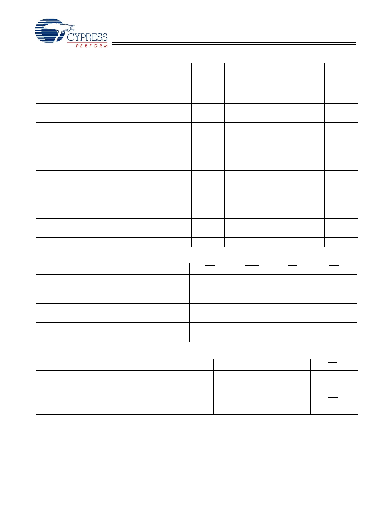
Truth Table for Read/Write[4]
Function (CY7C1480V33)
GW
Read
H
Read
H
Write Byte A – (DQA and DQPA)
H
Write Byte B – (DQB and DQPB)
H
Write Bytes B, A
H
Write Byte C – (DQC and DQPC)
H
Write Bytes C, A
H
Write Bytes C, B
H
Write Bytes C, B, A
H
Write Byte D – (DQD and DQPD)
H
Write Bytes D, A
H
Write Bytes D, B
H
Write Bytes D, B, A
H
Write Bytes D, C
H
Write Bytes D, C, A
H
Write Bytes D, C, B
H
Write All Bytes
H
Write All Bytes
L
Truth Table for Read/Write[4]
Function (CY7C1482V33)
Read
Read
Write Byte A – (DQA and DQPA)
Write Byte B – (DQB and DQPB)
Write Bytes B, A
Write All Bytes
Write All Bytes
Truth Table for Read/Write[7]
Function (CY7C1486V33)
Read
Read
Write Byte x – (DQx and DQPx)
Write All Bytes
Write All Bytes
BWE
H
L
L
L
L
L
L
L
L
L
L
L
L
L
L
L
L
X
BWD
X
H
H
H
H
H
H
H
H
L
L
L
L
L
L
L
L
X
BWC
X
H
H
H
H
L
L
L
L
H
H
H
H
L
L
L
L
X
BWB
X
H
H
L
L
H
H
L
L
H
H
L
L
H
H
L
L
X
BWA
X
H
L
H
L
H
L
H
L
H
L
H
L
H
L
H
L
X
GW
BWE
BWB
BWA
H
H
X
X
H
L
H
H
H
L
H
L
H
L
L
H
H
L
L
L
H
L
L
L
L
X
X
X
GW
BWE
BWX
H
H
X
H
L
All BW = H
H
L
L
H
L
All BW = L
L
X
X
Note:
7. BWx represents any byte write signal BW[0..7].To enable any byte write BWx, a Logic LOW signal should be applied at clock rise.Any number of bye writes can
be enabled at the same time for any given write.
Document #: 38-05283 Rev. *G
Page 11 of 31
[+] Feedback
Share Link: 