56F801 データシートの表示(PDF) - Motorola => Freescale
部品番号
コンポーネント説明
メーカー
56F801 Datasheet PDF : 44 Pages
| |||
Freescale Semiconductor, Inc.
JTAG/OnCE
2.10 JTAG/OnCE
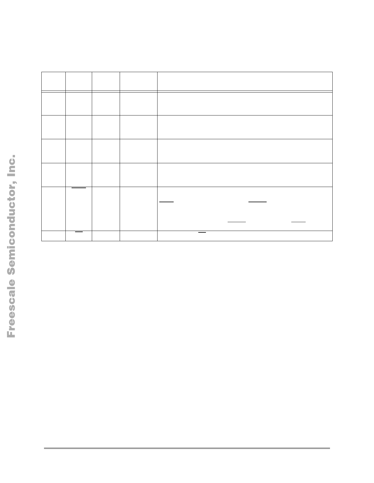
Table 13. JTAG/On-Chip Emulation (OnCE) Signals
No. of
Pins
1
1
1
1
1
1
Signal Signal State During
Name Type
Reset
Signal Description
TCK
TMS
TDI
TDO
TRST
DE
Input Input, pulled Test Clock Input—This input pin provides a gated clock to
(Schmitt) low internally synchronize the test logic and shift serial data to the JTAG/OnCE port.
The pin is connected internally to a pull-down resistor.
Input Input, pulled Test Mode Select Input—This input pin is used to sequence the JTAG
(Schmitt) high internally TAP controller’s state machine. It is sampled on the rising edge of TCK
and has an on-chip pull-up resistor.
Input Input, pulled Test Data Input—This input pin provides a serial input data stream to
(Schmitt) high internally the JTAG/OnCE port. It is sampled on the rising edge of TCK and has
an on-chip pull-up resistor.
Output
Tri-stated
Test Data Output—This tri-statable output pin provides a serial output
data stream from the JTAG/OnCE port. It is driven in the Shift-IR and
Shift-DR controller states, and changes on the falling edge of TCK.
Input Input, pulled Test Reset—As an input, a low signal on this pin provides a reset
(Schmitt) high internally signal to the JTAG TAP controller. To ensure complete hardware reset,
TRST should be asserted whenever RESET is asserted. The only
exception occurs in a debugging environment when a hardware device
reset is required and it is necessary not to reset the OnCE/JTAG
module. In this case, assert RESET, but do not assert TRST.
Output
Output Debug Event—DE provides a low pulse on recognized debug events.
Part 3 Specifications
3.1 General Characteristics
The 56F801 is fabricated in high-density CMOS with 5-volt tolerant TTL-compatible digital inputs. The
term “5-volt tolerant” refers to the capability of an I/O pin, built on a 3.3V compatible process technology,
to withstand a voltage up to 5.5V without damaging the device. Many systems have a mixture of devices
designed for 3.3V and 5V power supplies. In such systems, a bus may carry both 3.3V and 5V- compatible
I/O voltage levels (a standard 3.3V I/O is designed to receive a maximum voltage of 3.3V ± 10% during
normal operation without causing damage). This 5V-tolerant capability therefore offers the power savings
of 3.3V I/O levels while being able to receive 5V levels without being damaged.
Absolute maximum ratings given in Table 14 are stress ratings only, and functional operation at the
maximum is not guaranteed. Stress beyond these ratings may affect device reliability or cause permanent
damage to the device.
The 56F801 DC and AC electrical specifications are preliminary and are from design simulations. These
specifications may not be fully tested or guaranteed at this early stage of the product life cycle. Finalized
specifications will be published after complete characterization and device qualifications have been
completed.
56F801 Technical Data
11
For More Information On This Product,
Go to: www.freescale.com
Share Link: 